ALL ABOUT FLEX PCB
-
Read more: PCB Development – You May Not Know About The Future Trends!
Introduction to PCB Development and Emerging Trends Printed Circuit Boards (PCBs) are the backbone of modern electronics. These thin boards made of fiberglass or composite material provide mechanical support and electrical connections for electronic components using conductive pathways, tracks, or signal traces etched from copper sheets. PCBs have revolutionized the electronics industry by enabling the…
-
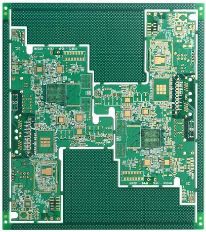
 Read more: How to Determine if Your Product is HDI or A Regular PCB Board
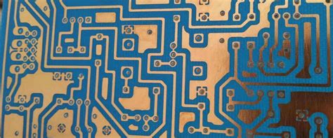
What is a Regular PCB? A regular PCB, also known as a conventional PCB, is a printed circuit board that consists of conductive tracks, pads, and other features etched from copper sheets laminated onto a non-conductive substrate. These boards are used to mechanically support and electrically connect electronic components using conductive pathways, tracks, or signal…
-
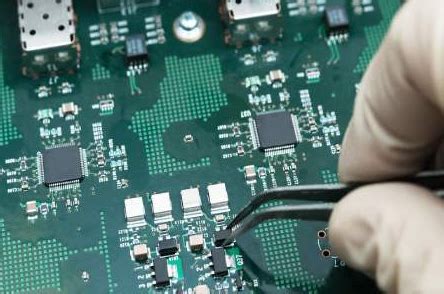
Automated X ray Inspection AXI
Posted by
–
 Read more: Automated X ray Inspection AXI
How AXI Works X-ray Imaging Principles AXI systems work by generating X-rays and directing them through the PCBA being inspected. As X-rays pass through the board, they are attenuated differently depending on the density and thickness of the materials they encounter. Denser materials like metals absorb more X-rays compared to less dense materials like plastics…
-
 Read more: Circuit Board Repair Kit Tape and Pad PCB fabrication
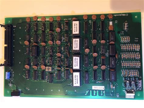
What is PCB Fabrication? PCB fabrication is the process of designing and manufacturing printed circuit boards (PCBs). PCBs are essential components in electronic devices, serving as the foundation for connecting and supporting various electronic components. The fabrication process involves several steps, including design, material selection, etching, drilling, and finishing. Steps in PCB Fabrication Design Material…
-
How to Spray Photo Resist on PCB
Posted by
–
 Read more: How to Spray Photo Resist on PCB
Introduction to PCB Photoresist Printed Circuit Boards (PCBs) are essential components in modern electronics. They provide a reliable and efficient way to connect electronic components and create complex circuits. One crucial step in the PCB manufacturing process is applying photoresist, a light-sensitive material that helps transfer the desired circuit pattern onto the copper layer of…
-
 Read more: 7 Tips to Prepare Printed Circuit Board Assembly Documentation
Introduction to PCB Documentation Printed Circuit Board (PCB) assembly documentation is a crucial aspect of the electronics manufacturing process. It serves as a guide for the assembly team, ensuring that the PCB is assembled correctly and efficiently. Proper documentation helps to minimize errors, reduce manufacturing time, and improve overall product quality. In this article, we…
-
Low Volume PCB Assembly Process Ultimate Guide
Posted by
–
 Read more: Low Volume PCB Assembly Process Ultimate Guide
Introduction to PCB Assembly Printed Circuit Board (PCB) assembly is the process of attaching electronic components to a PCB to create a functional electronic device. The PCB serves as the foundation for the electronic components, providing both mechanical support and electrical connectivity. Low volume PCB assembly refers to the production of a small number of…
-
 Read more: Blind Via PCB: 7 Key Elements to Take You Know All About Blind Vias(2023)
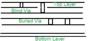
What is a Blind Via PCB? A blind via PCB, also known as a Buried Via PCB, is a type of printed circuit board (PCB) that has vias that are not visible on the surface of the board. These vias are used to connect different layers of the PCB without being exposed on the top…
-
DDR4 vs. DDR5 RAM: Will DDR5 Make a Difference?
Posted by
–
 Read more: DDR4 vs. DDR5 RAM: Will DDR5 Make a Difference?
Introduction Random access memory (RAM) is a critical component in any computer system. It acts as the computer’s short-term memory, storing data and instructions that the CPU needs to access quickly. As technology advances, so does the development of faster and more efficient RAM. The latest iteration of this technology is DDR5 RAM, which promises…
-
 Read more: Buried Via PCB: Here is what you need to know about this PCB type.
What is a Buried Via PCB? A Buried Via PCB, also known as a sub-surface mounted via PCB, is a type of printed circuit board that features vias that are buried within the inner layers of the board. Unlike traditional through-hole vias, which go through all layers of the PCB, buried vias only connect the…


