ALL ABOUT FLEX PCB
-
What is PCB Microsections
Posted by
–
Read more: What is PCB MicrosectionsIntroduction to PCB Microsections PCB microsections are a crucial technique used in the analysis and quality control of printed circuit boards (PCBs). This process involves cutting a small, representative sample of a PCB and examining it under a microscope to assess the quality of the board’s construction, identify potential defects, […]
-
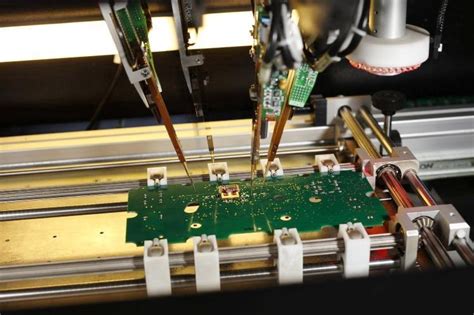
Selective Soldering
Posted by
–
 Read more: Selective Soldering
What is Selective Soldering? Selective soldering, also known as Selsoldering, is a process used in electronics manufacturing to solder specific components onto printed circuit boards (PCBs). Unlike wave soldering, which solders all components simultaneously, selective soldering targets individual components or groups of components, allowing for greater precision and flexibility in […]
-
 Read more: IPC-A-600 Acceptability of Printed Boards: Classes
Introduction to IPC-A-600 Standards IPC-A-600 is the industry standard for establishing acceptability requirements for printed circuit boards (PCBs). Developed by the Association Connecting Electronics Industries (IPC), this standard provides visual quality acceptability requirements and illustrations for PCBs. It covers various aspects of PCB manufacturing, including materials, workmanship, solderability, and surface […]
-
Blind and Buried Vias
Posted by
–
 Read more: Blind and Buried Vias
What are Blind-Buried-Vias? Blind and buried vias are two types of interconnects used in printed circuit board (PCB) design. These vias provide electrical connections between different layers of a multi-layer PCB, allowing for more complex and compact designs. Unlike through-hole vias, which span the entire thickness of the board, blind […]
-
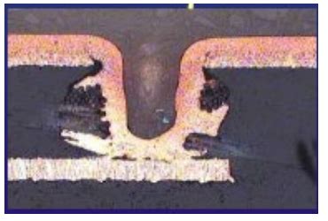
What is Pad to Pad (PP)?
Posted by
–
 Read more: What is Pad to Pad (PP)?
Why is Pad to Pad Spacing Important? Pad-to-Pad spacing plays a crucial role in several aspects of PCB design and manufacturing: 1. Component Placement The pad-to-pad distance directly affects the placement of components on the PCB. It determines how closely components can be placed next to each other without causing […]
-
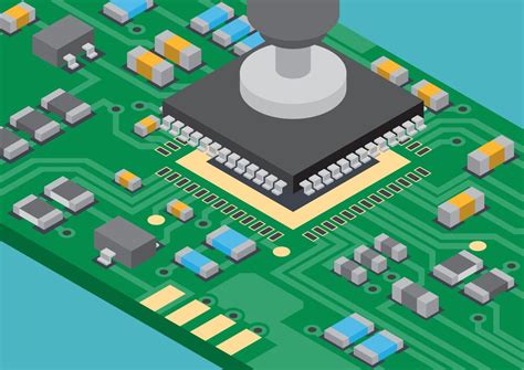
SMT Process Introduction
Posted by
–
 Read more: SMT Process Introduction
What is Surface-mount technology (SMT)? Surface-mount technology is a method of assembling electronic components directly onto the surface of a printed circuit board. Unlike through-hole technology (THT), where component leads are inserted into holes drilled in the PCB and soldered on the opposite side, SMT components are placed and soldered […]
-
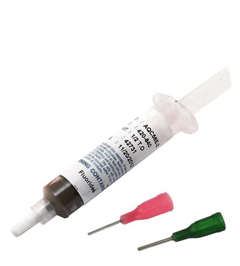 Read more: How to Choose, Store, and Use Solder Paste for Assembly
Introduction to Solder Paste Solder paste is a crucial component in the electronics assembly process, especially for Surface-mount technology (SMT). It is a mixture of tiny solder particles suspended in a flux medium, which helps to establish electrical and mechanical connections between electronic components and printed circuit boards (PCBs). Choosing […]
-
What is Cu (Copper)?
Posted by
–
 Read more: What is Cu (Copper)?
Properties of Copper Physical Properties Property Value Atomic Number 29 Atomic Mass 63.546 g/mol Density 8.96 g/cm³ Melting Point 1084.62°C Boiling Point 2562°C Specific Heat Capacity 0.385 J/(g·K) Thermal Conductivity 401 W/(m·K) Electrical Conductivity 5.96 × 10⁷ S/m Crystal Structure Face-Centered Cubic (FCC) Copper has a face-centered cubic crystal structure, […]
-
What About Underwriters Laboratory (UL)?
Posted by
–
 Read more: What About Underwriters Laboratory (UL)?
Table of Contents History of Underwriters Laboratory UL’s Mission and Purpose UL Standards and Certifications The UL Mark UL’s Testing Process UL’s Global Reach UL’s Impact on Consumer Safety UL’s Role in Sustainability UL’s Partnerships and Collaborations The Future of Underwriters Laboratory Frequently Asked Questions (FAQ) Request Flex PCB Manufacturing […]
-
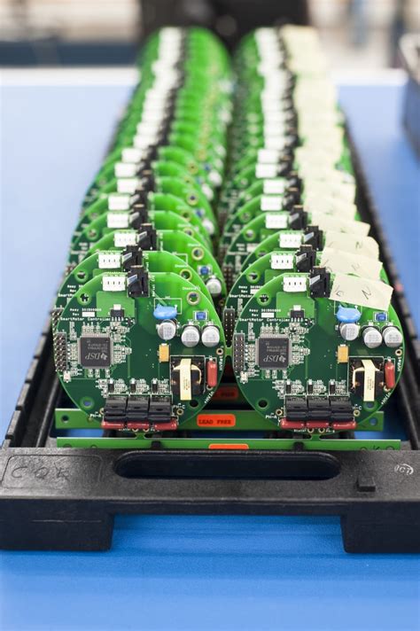 Read more: Printed Circuit Board Assembly Definition, Technology, and Uses
What is PCB Assembly? PCB assembly is the process of assembling electronic components onto a printed circuit board (PCB) to create a functional electronic device. The PCB is a flat board made of insulating materials, such as fiberglass or plastic, with conductive pathways etched onto its surface. These pathways, known […]


