Introduction to BJT Biasing
Bipolar Junction Transistors (BJTs) are essential components in electronic circuits, playing a crucial role in amplification and switching applications. To ensure proper operation and optimal performance of BJTs, it is necessary to understand the concept of biasing. BJT biasing involves setting the operating point of the transistor, which determines its quiescent current and voltage levels. In this comprehensive article, we will dive deep into the world of BJT biasing, covering various biasing techniques, their advantages, disadvantages, and practical considerations.
What is BJT Biasing?
BJT biasing refers to the process of establishing the desired operating point of a bipolar junction transistor in an electronic circuit. The operating point is determined by the DC voltage and current levels applied to the transistor’s terminals: the base, collector, and emitter. Proper biasing ensures that the transistor operates in the desired region, such as the active region for amplification or the saturation region for switching.
The primary objectives of BJT biasing are:
1. To set the quiescent point (Q-point) of the transistor, which is the steady-state operating point in the absence of an input signal.
2. To provide the necessary DC voltages and currents to the transistor’s terminals to maintain the desired operating region.
3. To ensure the stability of the operating point against variations in temperature, supply voltage, and transistor parameters.

Importance of BJT Biasing
Proper BJT biasing is crucial for several reasons:
-
Optimal Performance: Biasing the transistor correctly ensures that it operates in the desired region, such as the active region for amplification. This allows the transistor to provide the required gain, linearity, and frequency response.
-
Stability: Well-designed biasing circuits maintain a stable operating point despite variations in temperature, supply voltage, and transistor parameters. This stability is essential for reliable and consistent circuit operation.
-
Power Efficiency: Appropriate biasing helps to minimize power dissipation in the transistor, improving overall circuit efficiency. It prevents excessive current flow and ensures that the transistor operates within its safe operating area (SOA).
-
Signal Integrity: Proper biasing minimizes distortion and maintains the integrity of the input signal as it is amplified or processed by the transistor. It prevents clipping, saturation, or cutoff of the signal.

Types of BJT Biasing
There are several types of BJT biasing techniques, each with its own characteristics and applications. Let’s explore some of the most common biasing methods.
Fixed Bias
Fixed bias, also known as base bias, is the simplest BJT biasing technique. It involves applying a fixed DC voltage to the base of the transistor through a resistor. The base resistor limits the base current, which in turn determines the collector current.
Advantages:
– Simple and easy to implement
– Requires minimal components
Disadvantages:
– Poor stability against temperature variations
– Sensitive to variations in transistor parameters
– Limited control over the operating point
Emitter Bias
Emitter bias, also called self-bias, utilizes a resistor in the emitter circuit to provide negative feedback and improve stability. The emitter resistor helps to stabilize the operating point by compensating for changes in the base-emitter voltage.
Advantages:
– Improved stability compared to fixed bias
– Automatic compensation for variations in transistor parameters
– Simple to design and implement
Disadvantages:
– Reduced voltage swing due to the voltage drop across the emitter resistor
– Slight reduction in gain due to negative feedback
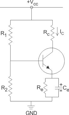
Voltage Divider Bias
Voltage divider bias is a popular biasing technique that offers good stability and control over the operating point. It uses a voltage divider network to set the base voltage and a series base resistor to limit the base current.
Advantages:
– Good stability against temperature variations
– Better control over the operating point
– Reduced sensitivity to transistor parameter variations
Disadvantages:
– Requires more components compared to fixed bias and emitter bias
– Slight reduction in gain due to the voltage divider network
Collector Feedback Bias
Collector feedback bias, also known as collector-to-base bias, employs a feedback resistor between the collector and base terminals. This feedback resistor provides negative feedback, which helps to stabilize the operating point.
Advantages:
– Improved stability compared to fixed bias
– Automatic compensation for variations in transistor parameters
– Simple to design and implement
Disadvantages:
– Reduced voltage swing due to the voltage drop across the feedback resistor
– Slight reduction in gain due to negative feedback
Comparison of BJT Biasing Techniques
| Biasing Technique | Stability | Complexity | Gain | Voltage Swing |
|---|---|---|---|---|
| Fixed Bias | Poor | Low | High | High |
| Emitter Bias | Moderate | Low | Moderate | Moderate |
| Voltage Divider Bias | Good | Moderate | Moderate | Moderate |
| Collector Feedback Bias | Moderate | Low | Moderate | Moderate |

Design Considerations for BJT Biasing
When designing BJT biasing circuits, several factors need to be considered to ensure optimal performance and reliability. Let’s discuss some key design considerations.
Quiescent Point (Q-Point) Selection
The quiescent point, or Q-point, represents the steady-state operating point of the transistor in the absence of an input signal. The choice of the Q-point depends on the desired operating region and the specific requirements of the circuit.
For amplification applications, the Q-point is typically set in the middle of the active region to allow maximum symmetrical voltage swing without clipping or distortion. This is achieved by selecting appropriate values for the Biasing Resistors and the supply voltage.
In switching applications, the Q-point is usually set in the saturation region to ensure that the Transistor Switches rapidly between the “on” and “off” states. This requires a sufficient base current to drive the transistor into saturation.
Stability and Temperature Compensation
Biasing circuits must be designed to maintain a stable operating point despite variations in temperature, supply voltage, and transistor parameters. Temperature changes can affect the base-emitter voltage and the collector current, leading to shifts in the operating point.
To compensate for temperature variations, techniques such as emitter degeneration and the use of temperature-compensated biasing networks can be employed. Emitter degeneration involves adding a resistor in series with the emitter, which provides negative feedback and helps to stabilize the operating point.
Temperature-compensated biasing networks, such as the bandgap reference, can be used to generate a temperature-independent reference voltage for biasing purposes. These networks typically utilize the complementary temperature coefficients of different transistors to cancel out temperature variations.
Bias Stability Factor (S)
The bias stability factor, denoted as S, is a measure of how well a biasing circuit maintains the operating point despite variations in transistor parameters. A smaller value of S indicates better stability.
The bias stability factor is defined as the ratio of the change in collector current (ΔIC) to the change in base current (ΔIB) caused by variations in transistor parameters:
S = ΔIC / ΔIB
A well-designed biasing circuit should have a low value of S, typically less than 10, to ensure good stability.
Thermal Runaway and Safe Operating Area (SOA)
Thermal runaway is a condition where an increase in temperature leads to an increase in collector current, which further increases the temperature, creating a positive feedback loop. If not properly addressed, thermal runaway can cause excessive power dissipation and damage to the transistor.
To prevent thermal runaway, biasing circuits must be designed to limit the collector current and ensure that the transistor operates within its safe operating area (SOA). The SOA is a graphical representation of the maximum voltage and current limits that the transistor can handle without damage.
Techniques such as current limiting, using heat sinks, and employing thermal shutdown circuits can help mitigate the risk of thermal runaway and protect the transistor.
Practical Examples and Applications
Now that we have covered the fundamentals of BJT biasing, let’s explore some practical examples and applications.
Example 1: Common Emitter Amplifier with Voltage Divider Bias
A common emitter amplifier is a popular configuration for voltage amplification. In this example, we will design a common emitter amplifier using voltage divider bias.
Given:
– Supply voltage (VCC) = 12 V
– Desired quiescent collector current (ICQ) = 2 mA
– Desired quiescent collector-emitter voltage (VCEQ) = 6 V
– Transistor beta (β) = 100
Step 1: Calculate the required base current (IBQ) and base-emitter voltage (VBEQ).
IBQ = ICQ / β = 2 mA / 100 = 20 µA
VBEQ ≈ 0.7 V (assuming silicon transistor)
Step 2: Choose the voltage divider resistors (R1 and R2) to set the base voltage (VBQ).
VBQ = VBEQ + 0.7 V = 1.4 V (providing some margin for stability)
Assume R2 = 10 kΩ
R1 = (VCC – VBQ) × R2 / VBQ = (12 V – 1.4 V) × 10 kΩ / 1.4 V ≈ 75.7 kΩ
Choose a standard value of 75 kΩ for R1.
Step 3: Calculate the emitter resistor (RE) to set the desired collector current.
RE = (VCC – VCEQ – VBEQ) / ICQ = (12 V – 6 V – 0.7 V) / 2 mA = 2.65 kΩ
Choose a standard value of 2.7 kΩ for RE.
Step 4: Calculate the collector resistor (RC) to set the desired collector-emitter voltage.
RC = (VCC – VCEQ) / ICQ = (12 V – 6 V) / 2 mA = 3 kΩ
The designed common emitter amplifier with voltage divider bias will have the following component values:
– R1 = 75 kΩ
– R2 = 10 kΩ
– RE = 2.7 kΩ
– RC = 3 kΩ
This biasing configuration provides good stability and allows for proper amplification of the input signal.
Example 2: Switching Circuit with Fixed Bias
In this example, we will design a switching circuit using fixed bias to turn a load on and off based on an input signal.
Given:
– Supply voltage (VCC) = 5 V
– Load resistance (RL) = 100 Ω
– Transistor saturation voltage (VCE(sat)) = 0.2 V
– Transistor beta (β) = 100
– Input signal: 0 V (low) to 5 V (high)
Step 1: Determine the required collector current (IC) to drive the load.
IC = (VCC – VCE(sat)) / RL = (5 V – 0.2 V) / 100 Ω = 48 mA
Step 2: Calculate the required base current (IB) to saturate the transistor.
IB = IC / β = 48 mA / 100 = 0.48 mA
Step 3: Choose the base resistor (RB) to limit the base current when the input is high.
RB = (VCC – VBE) / IB = (5 V – 0.7 V) / 0.48 mA ≈ 8.96 kΩ
Choose a standard value of 8.2 kΩ for RB.
The designed switching circuit with fixed bias will have the following component values:
– RB = 8.2 kΩ
– RL = 100 Ω
When the input signal is low (0 V), the transistor will be in the cut-off region, and the load will be turned off. When the input signal is high (5 V), the transistor will be saturated, and the load will be turned on.
Frequently Asked Questions (FAQ)
-
What is the purpose of biasing a BJT?
The purpose of biasing a BJT is to set the desired operating point (quiescent point) of the transistor, ensuring that it operates in the desired region (active or saturation) and provides the required performance characteristics such as gain, linearity, and stability. -
What are the different types of BJT biasing techniques?
The different types of BJT biasing techniques include fixed bias, emitter bias, voltage divider bias, and collector feedback bias. Each technique has its own advantages and disadvantages in terms of stability, complexity, gain, and voltage swing. -
Why is stability important in BJT biasing?
Stability is important in BJT biasing to ensure that the operating point remains consistent despite variations in temperature, supply voltage, and transistor parameters. A stable biasing circuit maintains the desired performance characteristics and prevents undesired behavior such as distortion or thermal runaway. -
What is the role of the emitter resistor in BJT biasing?
The emitter resistor in BJT biasing provides negative feedback, which helps to stabilize the operating point. It compensates for changes in the base-emitter voltage and reduces the sensitivity of the collector current to variations in transistor parameters. -
How can thermal runaway be prevented in BJT biasing?
Thermal runaway can be prevented in BJT biasing by designing the biasing circuit to limit the collector current and ensure that the transistor operates within its safe operating area (SOA). Techniques such as current limiting, using heat sinks, and employing thermal shutdown circuits can help mitigate the risk of thermal runaway.
Conclusion
BJT biasing is a critical aspect of designing electronic circuits that utilize bipolar junction transistors. Proper biasing ensures that the transistor operates in the desired region, provides the required performance characteristics, and maintains stability against variations in temperature, supply voltage, and transistor parameters.
In this article, we explored the fundamentals of BJT biasing, including the different biasing techniques, design considerations, and practical examples. We discussed the advantages and disadvantages of fixed bias, emitter bias, voltage divider bias, and collector feedback bias. We also covered important concepts such as quiescent point selection, stability, bias stability factor, thermal runaway, and safe operating area.
By understanding the principles of BJT biasing and applying the appropriate techniques, designers can create robust and reliable electronic circuits that meet the desired specifications. Whether it’s for amplification or switching applications, proper BJT biasing is essential for optimal performance and longevity of the circuit.
As you embark on your journey in electronics design, keep in mind the importance of BJT biasing and the various techniques at your disposal. Experiment with different biasing methods, analyze their behavior, and choose the most suitable approach for your specific application. With a solid understanding of BJT biasing, you’ll be well-equipped to design efficient and reliable electronic circuits.


Leave a Reply