Introduction to SMT Stencil
Surface Mount Technology (SMT) has revolutionized the electronics manufacturing industry by enabling the production of smaller, faster, and more reliable electronic devices. One of the critical components in the SMT assembly process is the stencil, which is used to apply solder paste onto the printed circuit board (PCB) before placing the components. SMT stencils play a crucial role in ensuring the accuracy, consistency, and quality of the solder paste deposition, which directly impacts the overall performance and reliability of the final product.
In this article, we will explore the various benefits of using SMT stencils in the electronics manufacturing process, including improved accuracy, increased efficiency, cost savings, and enhanced product quality. We will also discuss the different types of SMT stencils available, their applications, and best practices for selecting and using them effectively.
What is an SMT Stencil?
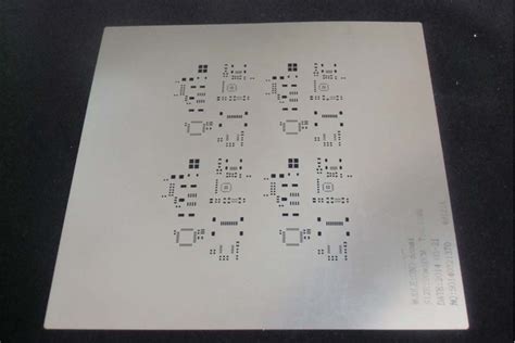
An SMT stencil is a thin, flat sheet of metal or other material with precise openings or apertures that correspond to the solder pad locations on a PCB. The stencil is placed over the PCB, and solder paste is applied using a squeegee or automated paste dispensing system. The solder paste is forced through the openings in the stencil onto the PCB pads, creating a precise and consistent deposit of solder paste on each pad.
SMT stencils are typically made from stainless steel, brass, or nickel, although other materials such as polyimide or laser-cut plastic may be used for specific applications. The thickness of the stencil varies depending on the size and pitch of the components being assembled, with thinner stencils used for finer pitch components and thicker stencils for larger components.

Benefits of Using SMT Stencils
1. Improved Accuracy and Consistency
One of the primary benefits of using SMT stencils is the improved accuracy and consistency of solder paste deposition. By using a stencil with precise aperture sizes and locations, the amount of solder paste applied to each pad can be carefully controlled, ensuring that the correct volume of paste is deposited every time. This consistency is critical for achieving reliable solder joints and preventing defects such as bridging, insufficient solder, or solder balls.
SMT stencils also help to maintain consistent solder paste height and shape across the entire PCB, which is essential for proper component placement and reflow. With the use of a stencil, the solder paste is deposited evenly and uniformly, reducing the risk of component misalignment or tombstoning during the reflow process.
2. Increased Efficiency and Productivity
Another significant benefit of using SMT stencils is the increased efficiency and productivity of the assembly process. By automating the solder paste application process with a stencil, the time and labor required for manual solder paste dispensing can be greatly reduced. This automation allows for faster cycle times, higher throughput, and reduced operator fatigue.
Additionally, the use of SMT stencils enables the assembly of high-density PCBs with fine-pitch components, which would be extremely challenging or impossible to achieve with manual solder paste application methods. The precision and repeatability of the stencil printing process allow for the reliable assembly of complex, high-performance electronic devices.
3. Cost Savings
Using SMT stencils can also result in significant cost savings for electronics manufacturers. By reducing the time and labor required for solder paste application, manufacturers can lower their production costs and increase their overall profitability. The increased efficiency and productivity enabled by SMT stencils also contribute to cost savings by allowing for faster time-to-market and reduced inventory costs.
Furthermore, the improved accuracy and consistency of solder paste deposition with SMT stencils help to reduce the number of defects and rework required, which can be a significant cost savings in terms of materials, labor, and production delays. The use of stencils also helps to minimize solder paste waste, as the precise aperture sizes ensure that only the necessary amount of paste is applied to each pad.
4. Enhanced Product Quality and Reliability
Perhaps the most important benefit of using SMT stencils is the enhanced product quality and reliability that results from the improved accuracy and consistency of solder paste deposition. With the correct volume and placement of solder paste on each pad, the risk of solder joint defects such as bridging, insufficient solder, or solder balls is greatly reduced. This leads to higher yields, fewer field failures, and improved customer satisfaction.
The consistent solder paste height and shape achieved with SMT stencils also contribute to better component placement and reflow, reducing the occurrence of component misalignment, tombstoning, or other assembly defects. By ensuring reliable and robust solder joints, SMT stencils help to improve the overall performance, durability, and longevity of the final product.

Types of SMT Stencils
There are several types of SMT stencils available, each with its own advantages and applications. The most common types include:
1. Laser-cut Stainless Steel Stencils
Laser-cut stainless steel stencils are the most widely used type of SMT stencil due to their durability, precision, and versatility. These stencils are created by using a high-powered laser to cut the apertures into a thin sheet of stainless steel. The laser cutting process allows for extremely precise and consistent aperture sizes and locations, making these stencils ideal for high-volume production and fine-pitch applications.
Stainless steel stencils are also highly durable and can withstand repeated use and cleaning without deformation or wear. They are compatible with a wide range of solder paste formulations and can be easily customized to accommodate unique PCB designs or component layouts.
2. Electroformed Nickel Stencils
Electroformed nickel stencils are created by electroplating nickel onto a master pattern, resulting in a thin, flexible stencil with highly accurate and consistent apertures. These stencils are typically used for applications requiring very fine pitch or high aspect ratio apertures, as the electroforming process allows for the creation of smaller and more precise openings than traditional laser cutting.
Nickel stencils are also known for their excellent paste release characteristics, which can help to reduce solder paste waste and improve print quality. However, they are generally more expensive than Laser-Cut Stencils and may have a shorter lifespan due to the thinner material and increased flexibility.
3. Nano-coated Stencils
Nano-coated stencils are a relatively new technology that involves applying a thin, nano-scale coating to the surface of a traditional laser-cut or electroformed stencil. The coating is designed to improve the solder paste release characteristics of the stencil, reducing the amount of paste that sticks to the aperture walls and improving the consistency of the paste deposit.
Nano-coated stencils can be particularly beneficial for applications using fine-pitch components or solder pastes with high viscosity or low slump. The improved paste release can help to reduce bridging, solder balls, and other print defects, while also extending the stencil’s usable life by minimizing paste buildup and simplifying cleaning.

Selecting the Right SMT Stencil
Choosing the right SMT stencil for a given application involves considering several key factors, including:
1. Aperture Size and Pitch
The aperture size and pitch of the stencil must be carefully matched to the size and spacing of the solder pads on the PCB. In general, smaller apertures and finer pitch require thinner stencils and more precise printing processes to achieve reliable paste deposition. It’s essential to work closely with the stencil manufacturer and follow industry guidelines to determine the optimal aperture size and pitch for a given component and PCB layout.
2. Stencil Thickness
The thickness of the stencil directly affects the volume of solder paste deposited on each pad. Thicker stencils will deposit more paste, while thinner stencils will deposit less. The appropriate stencil thickness depends on factors such as the size and pitch of the components, the solder paste properties, and the desired solder joint profile. A general rule of thumb is to use a stencil thickness that is 80-90% of the smallest aperture width, although this may vary depending on the specific application.
3. Material and Durability
The choice of stencil material should be based on the specific requirements of the application, including the production volume, solder paste type, and cleaning process. Stainless steel stencils are the most common choice for high-volume production due to their durability and compatibility with a wide range of solder pastes. Nickel stencils may be preferred for very fine-pitch applications, while nano-coated stencils can offer improved paste release and print quality.
4. Aperture Design and Layout
The design and layout of the stencil apertures can have a significant impact on the quality and consistency of the solder paste deposit. Factors such as aperture shape, wall angle, and aspect ratio must be carefully considered to ensure optimal paste release and print quality. Additionally, the stencil layout should be optimized to minimize solder paste waste and ensure even distribution of paste across the PCB.
Best Practices for Using SMT Stencils
To achieve the best results with SMT stencils, it’s important to follow some key best practices:
1. Proper Stencil Handling and Storage
SMT stencils should be handled with care to avoid damage or contamination. Always wear gloves when handling stencils, and store them in a clean, dry environment when not in use. Stencils should be inspected regularly for signs of wear, damage, or paste buildup, and replaced or cleaned as necessary to maintain optimal performance.
2. Regular Cleaning and Maintenance
Regular cleaning and maintenance of SMT stencils are essential to ensure consistent print quality and extend the stencil’s usable life. Solder paste residue and other contaminants can build up on the stencil over time, affecting the aperture size and shape and reducing paste release. Stencils should be cleaned frequently using appropriate solvents and methods, following the manufacturer’s recommendations and industry best practices.
3. Proper Alignment and Gasketing
Proper alignment and gasketing of the stencil to the PCB are critical for achieving accurate and consistent solder paste deposition. The stencil should be securely mounted in the printer and aligned to the PCB using fiducial marks or other reference points. Gasketing materials should be used to create a tight seal between the stencil and PCB, preventing paste bleed and ensuring even pressure distribution during printing.
4. Optimized Printing Parameters
The printing parameters, such as squeegee pressure, speed, and angle, should be carefully optimized for each specific application to achieve the best possible print quality. Factors such as solder paste type, stencil thickness, and aperture design will all affect the optimal printing parameters. It may be necessary to conduct extensive testing and experimentation to determine the ideal settings for a given application.
Frequently Asked Questions (FAQ)
1. What is the difference between a stencil and a screen in SMT assembly?
A stencil is a thin, flat sheet of metal with precise openings or apertures that correspond to the solder pad locations on a PCB. Solder paste is applied through the stencil onto the PCB pads. In contrast, a screen is a mesh stretched over a frame, with a stencil-like pattern applied to the mesh. Screens are typically used for larger, coarser-pitch components and may be preferred for certain solder paste formulations or applications.
2. How often should SMT stencils be cleaned?
The frequency of stencil cleaning depends on factors such as the solder paste type, printing volume, and environmental conditions. In general, stencils should be cleaned at least once per shift or every 4-8 hours of continuous printing. However, more frequent cleaning may be necessary for high-volume production or when using solder pastes with a tendency to dry or harden quickly.
3. Can SMT stencils be reused?
Yes, SMT stencils can be reused multiple times with proper cleaning and maintenance. The lifespan of a stencil depends on factors such as the material, thickness, and aperture design, as well as the cleaning and handling procedures. Stainless steel stencils are known for their durability and can often be used for thousands of prints before needing replacement.
4. How do I choose the right solder paste for my SMT stencil?
The choice of solder paste should be based on factors such as the component size and pitch, PCB surface finish, reflow profile, and environmental requirements. The solder paste should have a particle size and viscosity that is compatible with the stencil aperture size and shape, as well as good printing and release characteristics. It’s essential to work closely with the solder paste manufacturer and conduct thorough testing to select the optimal paste for a given application.
5. What are some common causes of solder paste printing defects?
Some common causes of solder paste printing defects include:
- Incorrect stencil aperture size or design
- Improper stencil alignment or gasketing
- Solder paste contamination or degradation
- Incorrect printing parameters (pressure, speed, angle)
- PCB surface contamination or oxidation
- Environmental factors (temperature, humidity)
By understanding and addressing these potential issues, manufacturers can minimize printing defects and improve the overall quality and reliability of their SMT assembly process.
Conclusion
SMT stencils are a critical component in the electronics manufacturing process, offering numerous benefits including improved accuracy, increased efficiency, cost savings, and enhanced product quality. By selecting the right stencil type, material, and design for a given application and following best practices for handling, cleaning, and maintenance, manufacturers can optimize their solder paste printing process and achieve reliable, high-quality solder joints.
As the electronics industry continues to evolve and push the boundaries of miniaturization and performance, the role of SMT stencils in enabling these advancements will only become more important. By staying up-to-date with the latest stencil technologies and best practices, manufacturers can position themselves to meet the challenges and opportunities of the future.
| Stencil Type | Advantages | Disadvantages |
|---|---|---|
| Laser-cut Stainless Steel | – Durable and long-lasting – Precise and consistent apertures – Compatible with a wide range of solder pastes |
– May be more expensive than other stencil types – Requires specialized cutting equipment |
| Electroformed Nickel | – Excellent for fine-pitch and high aspect ratio apertures – Good paste release characteristics |
– More expensive than laser-cut stencils – Shorter lifespan due to thinner material and increased flexibility |
| Nano-coated | – Improved paste release and print quality – Reduced bridging, solder balls, and other defects – Extended stencil life due to reduced paste buildup |
– Higher initial cost than non-coated stencils – May require specialized cleaning processes |
In summary, SMT stencils are an essential tool for achieving accurate, efficient, and reliable solder paste printing in electronics manufacturing. By carefully selecting the right stencil type, material, and design, and following best practices for use and maintenance, manufacturers can unlock the full potential of their SMT assembly process and produce high-quality, high-performance electronic devices.


Leave a Reply