What is PCB Back Drilling?
PCB back drilling, also known as controlled depth drilling or back-drill, is a process used in the manufacturing of high-speed printed circuit boards (PCBs) to remove the unused portion of a plated through-hole (PTH) that extends beyond the last layer of the PCB. This technique is essential for reducing signal integrity issues, such as impedance discontinuities and signal reflections, which can occur in high-speed digital designs.
Why is PCB Back Drilling Necessary?
As the demand for faster data transmission rates and higher frequencies in electronic devices increases, PCB designers face challenges in maintaining signal integrity. One of the main issues arises from the presence of stub resonance in the unused portion of PTHs.
When a signal travels through a via (a type of PTH), it encounters an impedance discontinuity at the end of the via barrel, where the unused portion of the hole acts as a stub. This stub can cause signal reflections and resonance, leading to signal distortion, increased insertion loss, and crosstalk. These issues become more pronounced at higher frequencies, making back drilling a crucial process for high-speed PCB designs.
Benefits of PCB Back Drilling
-
Improved Signal Integrity: By removing the unused portion of the via barrel, back drilling minimizes stub resonance and signal reflections, resulting in cleaner and more accurate signal transmission.
-
Reduced Insertion Loss: Back drilling helps reduce the insertion loss caused by the impedance discontinuity at the end of the via barrel, allowing for better signal propagation.
-
Enhanced Crosstalk Control: By eliminating the stub, back drilling reduces the coupling between adjacent vias, minimizing crosstalk and improving overall signal quality.
-
Increased Bandwidth: With improved signal integrity and reduced signal distortion, back drilling enables PCBs to support higher frequencies and faster data transmission rates.
How is PCB Back Drilling Performed?
The PCB back drilling process involves several steps to ensure accurate and precise removal of the unused portion of the via barrel. Here’s an overview of the back drilling process:
-
Design Preparation: The PCB design files are prepared for back drilling by identifying the vias that require the process and specifying the desired drill depth for each via.
-
Drill File Generation: A specialized drill file is created, containing the coordinates and depths for each back drill hole. This file is used to guide the drilling machine during the back drilling process.
-
PCB Alignment: The manufactured PCB is aligned on the drilling machine using fiducial marks or other reference points to ensure accurate positioning.
-
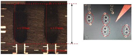
Back Drilling: The drilling machine uses the generated drill file to precisely drill the back side of the PCB, removing the unused portion of the via barrel up to the specified depth. High-speed spindles and small-diameter drill bits are used to minimize the risk of damaging the PCB or the via.
-
Cleaning: After back drilling, the PCB undergoes a cleaning process to remove any debris or burrs generated during the drilling process.
-
Inspection: The back drilled PCB is inspected to ensure that the process was performed accurately and that the desired stub length has been achieved.
Challenges in PCB Back Drilling
While back drilling offers significant benefits for high-speed PCB designs, there are some challenges associated with the process:
-
Accuracy: Back drilling requires precise control over the drilling depth to avoid damaging the PCB or the via. Inaccurate drilling can lead to incomplete stub removal or damage to the signal layers.
-
Increased Manufacturing Time and Cost: The additional back drilling step in the PCB manufacturing process increases the overall production time and cost compared to traditional PCB fabrication.
-
Limitations on Via Size and Spacing: Back drilling becomes more challenging as via sizes decrease and via density increases. Smaller vias require more precise drilling control and may limit the minimum achievable stub length.

PCB Back Drilling Design Considerations
To ensure successful back drilling and optimize the benefits of the process, PCB designers should consider the following factors when planning their high-speed designs:
Via Design
-
Via Size: Choose appropriate via sizes that balance the requirements for signal integrity and manufacturability. Smaller vias are more challenging to back drill accurately, while larger vias may consume more board space.
-
Via Placement: Position vias strategically to minimize the impact of stubs on signal integrity. Avoid placing vias in critical signal paths or near sensitive components whenever possible.
-
Via Stub Length: Determine the maximum allowable stub length based on the operating frequency and the desired signal integrity performance. Shorter stub lengths are generally preferred for high-speed designs.
Layer Stack-up
-
Signal Layer Arrangement: Optimize the layer stack-up to minimize the number of vias required for signal routing. Consider using blind and buried vias to reduce the need for back drilling.
-
Ground Planes: Incorporate ground planes adjacent to signal layers to provide a clean return path and minimize the impact of via stubs on signal integrity.
Drill Depth Control
-
Depth Uniformity: Ensure that the specified back drill depths are consistent across all vias to be back drilled. Variations in drill depth can lead to inconsistent stub lengths and impact signal integrity.
-
Tolerance Management: Consider the tolerances associated with the PCB manufacturing process when specifying back drill depths. Allow for adequate margin to account for fabrication variations.

Alternatives to PCB Back Drilling
While back drilling is a widely used technique for managing via stubs in high-speed PCB designs, there are alternative approaches that can be considered:
-
Blind and Buried Vias: Using blind and buried vias can eliminate the need for through-hole vias in certain layers, reducing the overall via stub length. However, this approach may increase manufacturing costs and complexity.
-
Via-in-Pad: Placing vias directly in component pads can help minimize via stub lengths, but it requires careful design and manufacturing considerations to ensure reliability.
-
High-Density Interconnect (HDI) PCBs: HDI PCB technologies, such as microvias and sequential lamination, can enable shorter via stubs and improved signal integrity without the need for back drilling.

Frequently Asked Questions (FAQ)
1. What is the purpose of PCB back drilling?
PCB back drilling is used to remove the unused portion of a plated through-hole (via) that extends beyond the last layer of the PCB. This process helps reduce signal integrity issues, such as stub resonance and signal reflections, which can occur in high-speed digital designs.
2. Is back drilling necessary for all PCB designs?
No, back drilling is not necessary for all PCB designs. It is primarily used in high-speed digital designs where signal integrity is critical. Lower-speed designs or designs with shorter via stubs may not require back drilling.
3. What are the benefits of PCB back drilling?
The benefits of PCB back drilling include improved signal integrity, reduced insertion loss, enhanced crosstalk control, and increased bandwidth. By removing the unused portion of the via barrel, back drilling minimizes stub resonance and signal reflections, resulting in cleaner and more accurate signal transmission.
4. How does back drilling affect the PCB manufacturing process?
Back drilling adds an additional step to the PCB manufacturing process, increasing the overall production time and cost compared to traditional PCB fabrication. It requires specialized drilling machines and precise control over drilling depth to ensure accurate stub removal without damaging the PCB or the vias.
5. Are there any alternatives to PCB back drilling?
Yes, there are alternatives to PCB back drilling, such as using blind and buried vias, via-in-pad design, or high-density interconnect (HDI) PCB technologies like microvias and sequential lamination. These approaches can help reduce via stub lengths and improve signal integrity without the need for back drilling, but they may come with their own design and manufacturing considerations.


Leave a Reply