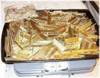
What are PCB Gold Fingers?
PCB gold fingers, also known as edge connector contacts or gold-plated contacts, are the gold-plated pads or traces located on the edge of a printed circuit board (PCB). These gold-plated contacts are designed to connect the PCB to another device or connector, enabling electrical signals and power to be transferred between them.
Gold fingers are commonly found on various types of PCBs, such as:
- Computer memory modules (e.g., RAM, ROM)
- Expansion cards (e.g., graphics cards, network cards)
- Mobile phone PCBs
- Game console cartridges
- Industrial equipment PCBs
Key Features of PCB Gold Fingers
-
Gold Plating: The contacts are plated with a thin layer of gold, which provides excellent electrical conductivity, corrosion resistance, and durability.
-
Precise Dimensions: Gold fingers are designed with precise dimensions to ensure a secure and reliable connection with the mating connector.
-
Multiple Contacts: PCBs can have multiple gold fingers, depending on the number of signals and power connections required.
-
Impedance Control: Gold fingers can be designed with controlled impedance to maintain signal integrity in high-speed applications.
Advantages of Using Gold for PCB Fingers
Gold is the preferred material for PCB edge connector contacts due to its unique properties and benefits:
1. Excellent Electrical Conductivity
Gold is an excellent electrical conductor, ensuring reliable signal transmission and low contact resistance. This is particularly important for high-frequency and low-voltage applications.
2. Corrosion Resistance
Gold is highly resistant to corrosion, oxidation, and tarnishing. This property helps maintain the integrity of the electrical connection over time, even in harsh environments.
3. Durability and Wear Resistance
Gold-plated contacts are highly durable and resistant to wear and tear. This is crucial for applications that require frequent insertion and removal of the PCB, such as memory modules or expansion cards.
4. Compatibility with Various Mating Connectors
Gold fingers are compatible with a wide range of mating connectors, including gold-plated and tin-plated connectors. This versatility allows PCBs with gold fingers to be used in various applications and systems.

Gold Finger Plating Process
The gold finger plating process involves several steps to ensure a high-quality and durable finish:
-
Base Copper Plating: A layer of copper is plated onto the PCB substrate to create the conductive traces and pads.
-
Nickel Plating: A layer of nickel is plated over the copper layer to provide a barrier between the copper and the gold. This prevents the formation of intermetallic compounds that can weaken the connection.
-
Gold Plating: Finally, a thin layer of gold is plated over the nickel layer. The gold plating thickness typically ranges from 0.05 to 0.5 micrometers (μm), depending on the application requirements.
| Plating Layer | Thickness Range (μm) |
|---|---|
| Copper | 25 – 70 |
| Nickel | 1 – 5 |
| Gold | 0.05 – 0.5 |
Gold Finger Plating Methods
There are two primary methods for gold finger plating:
-
Electroplating: This method involves applying an electrical current to deposit the gold onto the nickel surface. Electroplating offers good control over the plating thickness and uniformity.
-
Immersion (Electroless) Plating: In this method, the PCB is immersed in a gold plating solution, and the gold is deposited onto the nickel surface through a chemical reaction. Immersion plating is simpler and more cost-effective than electroplating but may result in a thinner and less uniform gold layer.

Designing PCBs with Gold Fingers
When designing PCBs with gold fingers, several factors must be considered to ensure optimal performance and reliability:
1. Contact Pitch and Spacing
The contact pitch and spacing should be designed according to the mating connector requirements and industry standards. Common pitches for gold fingers include:
- 1.27 mm (0.05 inches)
- 2.54 mm (0.1 inches)
2. Contact Dimensions
The gold finger dimensions, such as length, width, and thickness, should be designed to ensure a secure and reliable connection with the mating connector. The dimensions may vary depending on the application and connector type.
3. Impedance Control
For high-speed applications, the gold fingers should be designed with controlled impedance to maintain signal integrity. This involves carefully selecting the dielectric material, trace width, and spacing to achieve the desired characteristic impedance.
4. Solder Mask and Silkscreen
A solder mask should be applied to the PCB, leaving the gold fingers exposed. This helps protect the PCB from oxidation and prevents solder bridging during assembly. A silkscreen can be used to label the gold fingers for easy identification.

Testing and Quality Control
To ensure the quality and reliability of PCBs with gold fingers, several tests and inspections are performed:
1. Visual Inspection
Visual inspection is conducted to check for any defects or irregularities in the gold plating, such as discoloration, pitting, or peeling.
2. Thickness Measurement
The gold plating thickness is measured using X-ray fluorescence (XRF) or other non-destructive methods to ensure it meets the specified requirements.
3. Adhesion Test
An adhesion test, such as the tape test or scratch test, is performed to evaluate the bond strength between the gold layer and the underlying nickel layer.
4. Contact Resistance Measurement
The contact resistance between the gold fingers and the mating connector is measured to ensure it meets the specified limits. High contact resistance can lead to signal degradation and reliability issues.
5. Environmental Testing
PCBs with gold fingers may be subjected to various environmental tests, such as temperature cycling, humidity exposure, and salt spray tests, to assess their durability and reliability under different operating conditions.
Frequently Asked Questions (FAQ)
-
Q: What is the typical thickness of gold plating on PCB fingers?
A: The typical thickness of gold plating on PCB fingers ranges from 0.05 to 0.5 micrometers (μm), depending on the application requirements. -
Q: Can gold fingers be repaired if damaged?
A: In most cases, damaged gold fingers cannot be easily repaired. If the damage is extensive, the PCB may need to be replaced. -
Q: Are gold fingers compatible with lead-free solder processes?
A: Yes, gold fingers are compatible with lead-free solder processes. However, the gold plating thickness should be carefully controlled to prevent solder embrittlement. -
Q: Can gold fingers be used for high-current applications?
A: Gold fingers are primarily designed for low-current signal transmission. For high-current applications, thicker gold plating or alternative contact materials may be required. -
Q: How do I specify the gold finger requirements for my PCB design?
A: When specifying gold finger requirements, provide information such as the number of contacts, pitch, dimensions, plating thickness, and any specific standards or requirements. Consult with your PCB manufacturer for guidance on design and specifications.
Conclusion
PCB gold fingers play a crucial role in ensuring reliable and efficient electrical connections between PCBs and mating connectors. By understanding the key features, advantages, design considerations, and quality control aspects of gold fingers, engineers and designers can create high-performance PCBs for various applications.
When designing PCBs with gold fingers, it is essential to adhere to industry standards, select appropriate plating methods, and work closely with experienced PCB manufacturers to ensure the best results. Proper testing and quality control measures should also be implemented to guarantee the long-term reliability and durability of the gold-plated contacts.
As technology continues to advance, the demand for high-quality and reliable PCB gold fingers will remain strong. By staying informed about the latest developments and best practices in PCB gold finger design and manufacturing, engineers can create innovative and robust electronic devices that meet the ever-evolving needs of the industry.


Leave a Reply