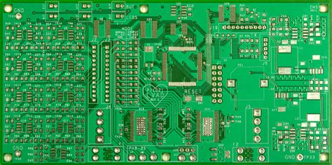
Introduction to PCB Layers
Printed Circuit Boards (PCBs) are essential components in modern electronics. They provide a platform for mounting and interconnecting electronic components, allowing for complex circuits to be designed and manufactured efficiently. One of the key aspects of PCB design is the use of layers. PCB layers are the different levels of conductive material that make up the board, each serving a specific purpose in the overall circuit design.
In this article, we will explore the various types of PCB layers, their functions, and how they contribute to the successful design and manufacture of PCBs for your project.
Types of PCB Layers
PCBs can be categorized based on the number of layers they contain. The most common types of PCBs are:
- Single-Layer PCBs
- Double-layer PCBs
- Multi-layer PCBs
Single-layer PCBs
Single-layer PCBs, also known as single-sided PCBs, have only one conductive layer. This layer is typically made of copper and is used for both component placement and signal routing. Single-layer PCBs are the simplest and most cost-effective type of PCB, making them ideal for basic, low-complexity projects.
Advantages of single-layer PCBs:
– Low cost
– Easy to design and manufacture
– Suitable for simple circuits
Disadvantages of single-layer PCBs:
– Limited routing options
– Not suitable for high-density designs
– Prone to electromagnetic interference (EMI)
Double-layer PCBs
Double-layer PCBs, also known as double-sided PCBs, have two conductive layers, one on each side of the board. These layers are connected using through-hole vias, which allow signals to pass from one layer to the other. Double-layer PCBs offer more routing options and higher component density compared to single-layer PCBs.
Advantages of double-layer PCBs:
– Increased routing options
– Higher component density
– Better signal integrity
– Reduced EMI
Disadvantages of double-layer PCBs:
– Higher cost compared to single-layer PCBs
– More complex design and manufacturing process
Multi-layer PCBs
Multi-layer PCBs have three or more conductive layers, with insulating layers separating them. The number of layers can vary depending on the complexity of the circuit and the desired performance. Multi-layer PCBs offer the highest component density and the most flexible routing options, making them suitable for complex, high-performance applications.
Advantages of multi-layer PCBs:
– High component density
– Excellent signal integrity
– Reduced EMI
– Improved thermal management
Disadvantages of multi-layer PCBs:
– High cost
– Complex design and manufacturing process
– Longer lead times
| PCB Type | Layers | Cost | Density | Complexity |
|---|---|---|---|---|
| Single-layer | 1 | Low | Low | Simple |
| Double-layer | 2 | Medium | Medium | Moderate |
| Multi-layer | 3+ | High | High | Complex |
Functions of PCB Layers
Each layer in a PCB serves a specific purpose in the overall circuit design. The most common types of layers and their functions are:
Signal Layers
Signal layers are used for routing electrical signals between components on the PCB. These layers are typically made of copper and are etched to create the desired circuit pattern. The number of signal layers in a PCB depends on the complexity of the circuit and the routing requirements.
In multi-layer PCBs, signal layers are often grouped in pairs, with one layer dedicated to horizontal routing and the other to vertical routing. This arrangement, known as orthogonal routing, helps minimize crosstalk and improve signal integrity.
Power and Ground Planes
Power and ground planes are used to distribute power and provide a reference ground for the circuit. These planes are typically solid copper layers that span the entire area of the PCB. By using dedicated power and ground planes, designers can ensure a stable and low-impedance power supply, reducing noise and improving overall circuit performance.
In multi-layer PCBs, power and ground planes are often placed on adjacent layers, separated by a thin insulating layer. This arrangement, known as a power-ground sandwich, helps minimize EMI and provide a low-inductance path for high-frequency currents.
Shielding Layers
Shielding layers are used to protect sensitive signals from external EMI and to prevent the circuit from emitting unwanted electromagnetic radiation. These layers are typically solid copper planes that are grounded, acting as a barrier between the circuit and the environment.
Shielding layers are often placed on the outer layers of the PCB, enclosing the signal and power layers. In some cases, additional shielding layers may be added between sensitive signal layers to provide further protection.

PCB Layer Stackup
The arrangement of layers in a PCB is known as the layer stackup. The layer stackup defines the order and spacing of the conductive and insulating layers, as well as the materials used for each layer. Proper layer stackup design is crucial for ensuring signal integrity, minimizing EMI, and meeting the mechanical and thermal requirements of the circuit.
When designing a layer stackup, consider the following factors:
-
Signal integrity: Ensure that sensitive signals are routed on appropriate layers and are adequately spaced from other signals and planes to minimize crosstalk and interference.
-
Power distribution: Place power and ground planes close to the components they serve to minimize inductance and ensure a stable power supply.
-
EMI: Use shielding layers and proper grounding techniques to minimize EMI and comply with electromagnetic compatibility (EMC) regulations.
-
Manufacturability: Consider the capabilities and limitations of your PCB manufacturer when designing the layer stackup, such as minimum trace width, spacing, and via size.
Here’s an example of a typical 4-layer PCB stackup:
| Layer | Function |
|---|---|
| Top | Signal, Components |
| Inner 1 | Ground Plane |
| Inner 2 | Power Plane |
| Bottom | Signal, Components |

FAQ
-
Q: How do I choose the right number of layers for my PCB?
A: The number of layers in your PCB depends on the complexity of your circuit, the routing requirements, and the desired performance. Start with a single-layer or double-layer PCB for simple circuits and move to multi-layer PCBs for more complex designs that require higher component density and better signal integrity. -
Q: Can I mix different types of layers in a single PCB?
A: Yes, you can mix different types of layers in a single PCB. For example, you can have signal layers, power and ground planes, and shielding layers in the same PCB. The key is to arrange the layers in a way that optimizes signal integrity, power distribution, and EMI protection. -
Q: What materials are used for PCB layers?
A: The most common material used for PCB layers is copper, which is an excellent conductor of electricity. The copper layers are typically laminated onto an insulating substrate, such as FR-4, which is a glass-reinforced epoxy laminate. Other materials, such as aluminum or carbon fiber, may be used for specialized applications. -
Q: How do vias connect different layers in a PCB?
A: Vias are small holes drilled through the PCB that are plated with a conductive material, typically copper. They allow signals to pass from one layer to another, enabling more complex routing and higher component density. There are several types of vias, including through-hole vias, blind vias, and buried vias, each suited for different applications and layer stackups. -
Q: What is the importance of a well-designed layer stackup?
A: A well-designed layer stackup is crucial for ensuring the proper functioning and reliability of your PCB. It helps optimize signal integrity, minimize EMI, and ensure proper power distribution. A poorly designed layer stackup can lead to issues such as crosstalk, signal reflections, and power supply instability, which can compromise the performance and reliability of your circuit.

Conclusion
Understanding PCB layers is essential for designing and manufacturing reliable and high-performance electronic circuits. By familiarizing yourself with the different types of layers, their functions, and how they contribute to the overall PCB design, you can make informed decisions when planning your project.
When designing your PCB, consider the complexity of your circuit, the routing requirements, and the desired performance. Choose the appropriate number and type of layers, and pay close attention to the layer stackup to ensure optimal signal integrity, power distribution, and EMI protection.
By following best practices and working closely with your PCB manufacturer, you can create PCBs that meet your project’s requirements and exceed your expectations.


Leave a Reply