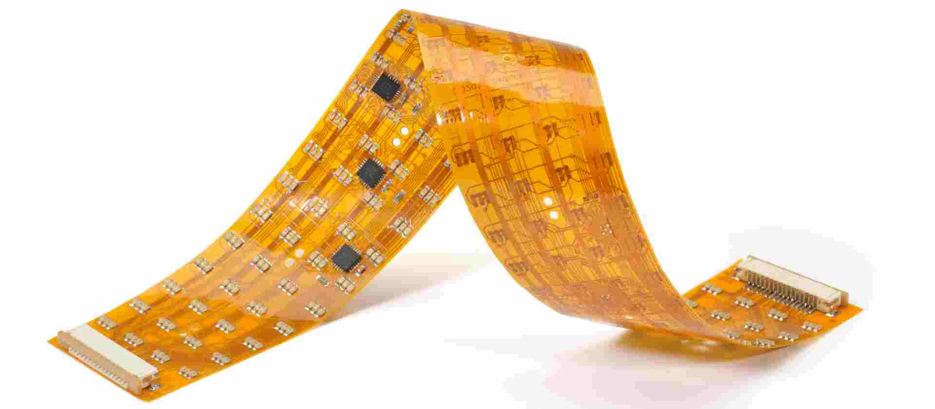
Flexible printed circuit boards (flex PCBs) offer many advantages over traditional rigid PCBs. They can bend and flex to fit into tight spaces, move dynamically in products, and improve reliability in high-vibration environments. However, flex PCBs require some unique design considerations. Follow these key tips when creating your flex PCB layout:
1. Plan for Controlled Impedance
Maintaining controlled impedance is critical for high-speed signals. Trace widths and dielectric materials significantly impact impedance.
- Use thinner dielectrics (1-3 mils) for tighter impedance tolerances.
- Wider traces increase impedance, narrower traces decrease it.
- Vary trace widths to match target impedance.
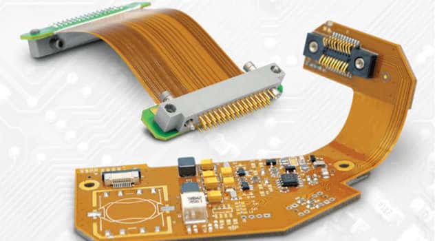
2. Minimize Stiffener Use
Stiffeners provide stability but inhibit flexibility. Use judiciously:
- Avoid when possible.
- Use selective stiffening at connectors/components.
- Polyimide and acrylic options available.
3. Design for Dynamic Flexing
Analyze required dynamic bending radii:
- Use larger bend radii to prevent conductor cracking.
- Radius requirements increase with more layers.
- Consider stress relief openings at flex points.
Typical Minimum Bend Radii
| Layers | Minimum Bend Radius |
|---|---|
| 1 | 0.075 in |
| 2 | 0.100 in |
| 4 | 0.150 in |
| 6 | 0.190 in |
4. Utilize Flex-Friendly Components
Select components suited for flexing:
- Prefer small surface-mount devices (SMDs).
- Avoid large, heavy through-hole components.
- Use flex-grade adhesive to secure components.
5. Manage Layer Stackup Carefully
Optimizing layer stackup prevents failures:
- Place components on inner layers to avoid cracking.
- Adhesive between layers provides shear support.
- Include coverlay over conductors for insulation.
6. Include Strain Relief
Accommodate bending forces with strain relief:
- Use openings/cutouts at transition points.
- Implement nested comb patterns.
- Avoid 90° angles.
7. Avoid Sharp Bends
Gradual bends last longer than sharp turns:
- Design with larger bend radii.
- Use combined arcs to form bend.
- Eliminate acute angles when possible.
8. Develop in Sections
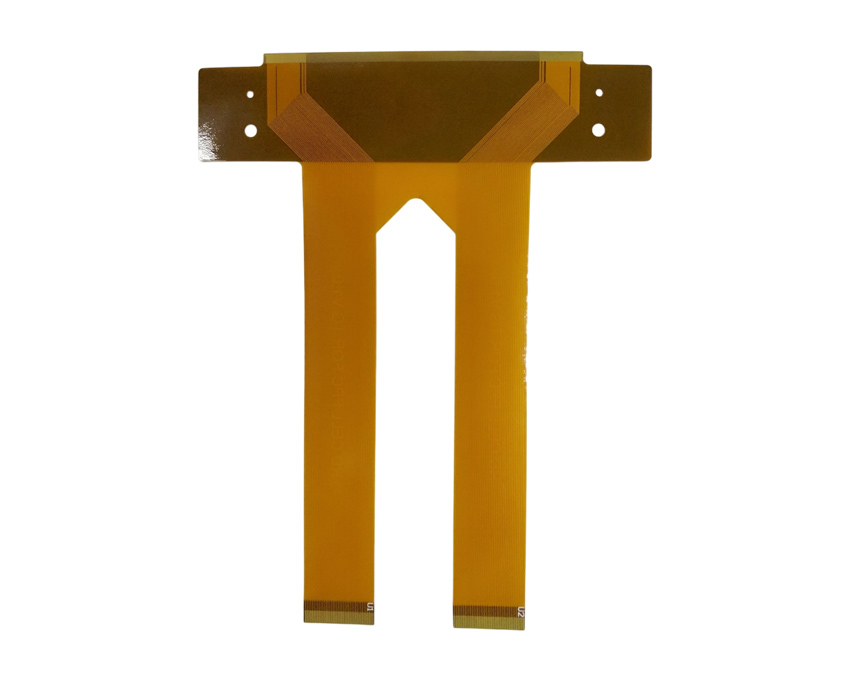
Design rigid sections connected by flex areas:
- Rigid sections for components and vias.
- Flex sections for dynamic movement.
- Combines advantages of both constructions.
9. Prototype and Test
Validate designs with prototypes:
- Test initial runs for real-world performance.
- Iterate on layouts to improve reliability.
- Refine bend radiuses, layer stackup, strain relief.
Following these guidelines will help you successfully design durable, high-performing flex PCBs. Don’t hesitate to consult experienced flex PCB designers or fabricators for guidance. With careful planning and prototyping, flex circuits can enhance and enable many innovative products.
Frequently Asked Questions
Q: What are the major benefits of using a flex PCB?
A: Flex PCBs offer several key advantages:
- Dynamic flexibility to fit and move within products
- Reliability in high vibration or flexing environments
- Lightweight, thin, and compact form factors
- Enhanced durability and fatigue resistance
- Reduced wiring and simpler assembly vs. wire harnesses
- Design freedom for curvature, bends, folding
Q: Are there limitations on the number of layers in flex PCBs?
A: Traditionally flex PCBs have been limited to 2 or 4 layers. However, advances in manufacturing and materials are enabling flex circuits with 6, 8, and even more layers, allowing for increased routing density. The main design considerations with more layers are maintaining minimum bend radii and managing layer stackup.
Q: What types of products commonly use flex PCBs?
A: Flex PCBs are found in many products where flexibility, space savings, or reliability are important factors. Some common examples include:
- Wearable devices
- Mobile phones
- Medical instruments
- Automotive electronics
- Industrial equipment
- Aerospace systems
Q: How durable are flex PCBs compared to rigid boards?
A: Properly designed flex PCBs can offer excellent durability and fatigue resistance exceeding traditional rigid PCBs. Key factors impacting flex life include:
- Bend radii – Larger radii improve life
- Strain relief – Openings at flex points reduce stress
- Layer stackup – Adhesive provides shear support
- Conductor design – Nested comb patterns add resilience
With optimal design, flex PCBs can survive over 100,000 dynamic flex cycles.
Q: What are some best practices for soldering components to flex PCBs?
A: Some tips for reliable soldering include:
- Use a lower temperature soldering iron to avoid damaging flex board or conductors.
- Keep component sizes and profiles small and low.
- Use solder masks defined lands for improved integrity.
- Stabilize boards during soldering to minimize flexing.
- Allow adequate cool down time to relieve stresses.
- Optical inspection ensures quality solder joints.


Leave a Reply