Introduction
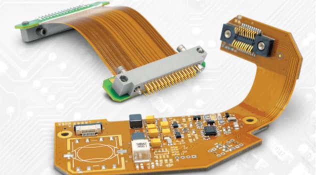
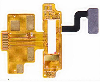
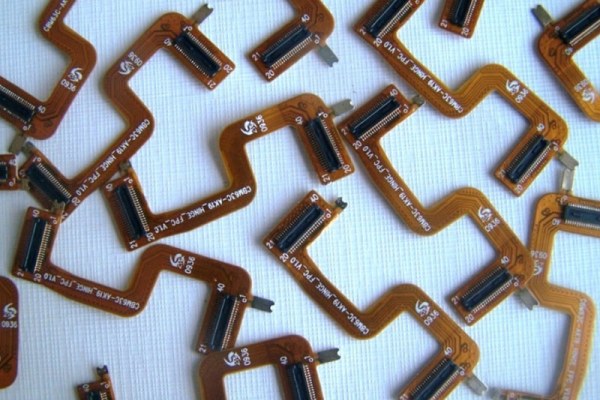
A flex PCB (flexible printed circuit board) is a type of PCB that can bend and flex. Flex PCBs are made of flexible insulating substrates like polyimide or polyester film. They are ideal for applications that require customized connections, space constraints, or dynamic flexing.
One key component of a flex PCB design is the stiffener. Stiffeners provide mechanical support and rigidity to the flex PCB, allowing it to maintain its shape during bending. In this article, we will provide an in-depth look at what stiffeners are, why they are used in flex PCBs, and the different types of stiffener materials and configurations.
What is a Stiffener?
A stiffener is a rigid material layer that is laminated onto or embedded within the flexible PCB substrate. The key functions of a stiffener are:
- Provide mechanical support – Stiffeners prevent sagging, wrinkling, and warping of the flex PCB when it undergoes bending and dynamic flexing. This helps maintain the designed shape and configuration.
- Reinforce solder connections – During assembly, a stiffener prevents damage to plated through holes (PTHs) and other solder joints on the flex PCB from the stresses of bending or vibration.
- Reduce flexible substrate elongation – The stiffener limits stretching of the flexible material when the PCB is bent repeatedly. This improves the reliability and lifespan of the flex PCB.
- Enable efficient PCB handling – Stiffeners make the flex PCB more rigid and easier to handle during fabrication, assembly, and installation. This avoids misalignment and improves process yields.
Why Use Stiffeners in Flex PCBs?
There are several important reasons why stiffeners are commonly used in flex PCB designs:
- Prevent failures – Stiffeners reduce mechanical stresses and prevent conductor cracking or delamination during dynamic bending and vibration. This improves reliability.
- Maintain shape – Rigid sections provided by stiffeners ensure that critical dimensions and alignments are maintained for components, connectors and contacts during flexing.
- Simplify assembly – Stiffeners make handling, loading, and assembly easier by providing stability and rigidity to flex PCB sections.
- Control bending – Strategic placement of stiffeners allows controlling where and how the flex PCB bends. Stiffeners can be used to create “hinges”.
- Reduce costs – Stiffeners allow using thinner, more economical flex materials without compromising reliability or shape retention.
Some common locations for stiffeners:
- High density component areas
- Connector zones
- Areas needing precise alignments
- Regions with tight bend radius requirements
Stiffener Materials
Several materials are used to fabricate stiffeners for flex PCBs:
Polyimide Film
- High strength, heat resistance, and flexibility
- Simple construction by laminating sheets of polyimide film onto flex PCB substrate
- Various thicknesses available (10μm to 125μm)
- Can cover entire surface or selectively laminated
Coverlay
- Photosensitive polymer that can be processed like solder mask -Applied in liquid form, exposed, and cured
- Provides good adhesion and some amount of stiffening
- Limited thickness up to around 30μm
Copper
- Plated or laminated copper foil, ranging from 12μm to 70μm thickness
- Excellent strength and rigidity
- Can be selectively patterned to form complex stiffener shapes
- Allows integration of thermal vias for heat dissipation
Stainless Steel
- High strength and rigidity
- Typically laminated in thinner sheets around 25μm to 50μm
- Provides good shielding against EMI/RFI
- Higher cost compared to other options
Aluminum
- Lightweight material with excellent rigidity
- Sheets laminated or metal backed dielectric used
- Complex stiffener shapes possible by precision etching
- Good thermal dissipation ability
- Cost effective option
Carbon Fiber
- Reinforced polymer composites with high stiffness and strength
- Allows very thin laminations to the order of 25μm with rigid support
- Low thermal expansion coefficient
- Relatively higher cost material
Stiffener Design Configurations
There are several design factors to consider when incorporating stiffeners in a flex PCB:
Stiffener Locations
Stiffeners can be located:
- On one side of the flex PCB substrate
- On both sides of the substrate
- Embedded internally between substrate layers
One-sided configurations are simplest, while double-sided allows maximum strengthening. Embedded stiffeners provide strengthening with minimal impact on flex circuit thickness.
Stiffener Extent
Stiffeners may:
- Run the complete length of the flex PCB
- Be localized in specific areas
- Form complex shapes around cutouts and openings
Full-length stiffeners provide overall rigidity, while localized stiffeners target high stress areas. Complex segmented stiffeners are possible using photolithographic patterning processes.
Stiffener Thickness
Typical stiffener thickness range:
- Polyimide: 10μm – 125μm
- Copper foil: 12μm – 70μm
- Stainless steel: 25μm – 50μm
Thicker stiffeners provide more rigidity at the expense of some flexibility. Copper and steel stiffeners also provide shielding against EMI/RFI.
Bonding Method
Stiffeners are attached by:
- Laminating sheets using adhesive
- Direct copper bonding without adhesive
- Coverlay materials that are coated and cured
Proper chemical treatment ensures reliable adhesion between the stiffening material and flexible substrate.
Bend Areas
No stiffeners are provided in areas of the flex PCB that need to bend. Minimum bend radius requirements must be factored into the stiffener layout. Openings in stiffeners may be provided to create flexible hinge points if needed.
Here is a summary comparison of common stiffener configurations:
| Configuration | Characteristics |
|---|---|
| Full-surface | Maximum rigidity, least flexibility |
| Selective | Targeted strengthening, moderate flexibility |
| Localized islands | Maximizes bending, provides limited strengthening |
| Remove in bend areas | Allows bending while still stiffening straight sections |
| Double-sided | Rigid support on both sides |
| Embedded | Internal strengthening with minimal thickness impact |
Considerations for Stiffener Design
Here are some best practices to consider when designing stiffeners:
- Place stiffeners along the entire length or width of connectors to prevent twisting or warping during mating.
- In high density BGA packages, use stiffeners under the package and surrounding solder joints to minimize stresses.
- Stiffeners around cutouts and openings prevent propagation of cracks and reinforce edges.
- Minimize number of discrete stiffener sections to reduce total flex circuit thickness.
- In double-sided boards, align stiffeners on both sides to maximize strengthening.
- Ensure minimum electrical clearance between stiffeners and adjacent conductors.
- Allow sufficient openings in stiffeners within bend areas to prevent cracking.
- Accommodate thermal expansion differences between stiffener and flex substrate materials.
- Account for stiffener thickness when calculating total flex stackup height.
With careful design and material selection, stiffeners can significantly improve the durability and reliability of dynamic flex PCBs.
Frequently Asked Questions (FQA):
Here are some common questions about stiffeners in flex PCBs:
Q1: Are stiffeners required for all flex PCB designs?
Not necessarily. Simple flex circuits without tight dynamic bending requirements may not need stiffeners. Stiffeners become more important for complex designs with dense components, smaller bend radii, or vigorous dynamic flexing.
Q2: Can you have a flex PCB without any stiffeners?
Yes, it is possible to have a flex PCB without any stiffeners. But the circuit needs to be relatively simple, with minimal components in the dynamic bending areas. Careful structural support to limit bending is also needed. Lack of stiffeners will limit the lifetime of such flex PCBs.
Q3: Where should stiffeners be located in a flex PCB?
Stiffeners should be placed in areas that undergo minimal bending but require strengthening. This includes connector zones, populated component sections, and areas around cutouts or openings. High stress areas prone to cracking also benefit from localized stiffener placement.
Q4: Can stiffeners be added to an existing flex PCB?
Yes, it is possible to add or enhance stiffeners for an already designed flex PCB through various techniques. These include laminating additional polyimide or metal foil layers, applying glass fabric reinforcements, or using coverlay materials. But redesigning the stiffeners from the start is recommended for optimal effectiveness.
Q5: How does the thickness of copper stiffeners affect flex PCB performance?
Thicker copper stiffeners provide greater rigidity, but reduce bendability. A good rule of thumb is to use thinner 12μm – 18μm copper for dynamic bending areas, and thicker 36μm – 70μm copper for stiff augmentation of connectors and populated regions. The width of copper stiffeners is also a factor, with narrower traces allowing more flex.
Conclusion
Stiffeners are critical components in flex PCB design. They strengthen the circuit and prevent failures while still allowing controlled bending. A variety of materials such as polyimide, coverlay, copper, and steel can be used. Careful analysis of mechanical requirements and liberal use of stiffeners in populated regions will result in robust, reliable flex PCB performance.


Leave a Reply