Why is PCB Tinning Important?
PCB tinning is essential for several reasons:
-
Protection against oxidation: Copper, the primary conductive material used in PCBs, is prone to oxidation when exposed to air. Oxidation can lead to poor solderability and reduced conductivity. Tinning the copper surfaces creates a barrier that prevents oxidation, ensuring better performance and longevity of the PCB.
-
Improved solderability: Tinned surfaces have better wettability, which means that molten solder can easily flow and adhere to the copper traces and pads. This results in stronger and more reliable solder joints during the assembly process.
-
Enhanced conductivity: Tinning helps to maintain the conductivity of the copper traces by preventing the formation of non-conductive oxide layers. This ensures that electrical signals can travel efficiently through the PCB without any interference or signal loss.
-
Increased shelf life: Tinned PCBs have a longer shelf life compared to non-tinned boards. The protective layer of solder prevents the copper from deteriorating over time, allowing you to store the PCBs for extended periods without compromising their quality.
Methods of PCB Tinning
There are several methods used for PCB tinning, each with its own advantages and disadvantages. Let’s explore the most common methods:
1. Hot Air Solder Leveling (HASL)
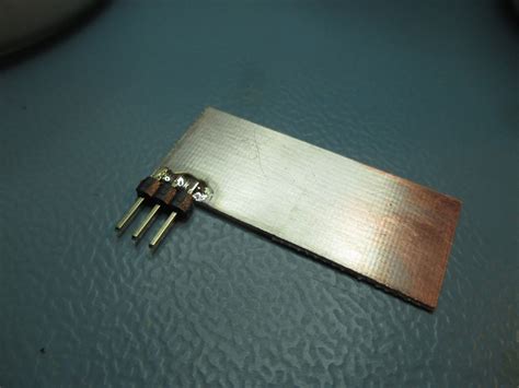
Hot Air Solder Leveling (HASL) is one of the most widely used methods for PCB tinning. In this process, the PCB is first immersed in a molten solder bath, which coats the copper surfaces with solder. Then, hot air is blown onto the board to level the solder and remove any excess. The resulting surface is flat and uniform, providing excellent solderability.
Advantages of HASL:
– Cost-effective
– Fast process
– Suitable for high-volume production
– Good solderability
Disadvantages of HASL:
– Uneven surface finish
– Potential for solder bridges
– Limited compatibility with fine-pitch components
2. Immersion Silver (ISV)
Immersion Silver (ISV) is a chemical process that deposits a thin layer of silver onto the copper surfaces of the PCB. The silver layer provides excellent solderability and protection against oxidation. ISV is often used as a lead-free alternative to HASL.
Advantages of ISV:
– Flat and uniform surface finish
– Suitable for fine-pitch components
– Excellent solderability
– Lead-free and RoHS compliant
Disadvantages of ISV:
– Higher cost compared to HASL
– Slower process
– Limited shelf life due to silver tarnishing
3. Electroless Nickel Immersion Gold (ENIG)
Electroless Nickel Immersion Gold (ENIG) is a two-step process that involves depositing a layer of nickel followed by a thin layer of gold onto the copper surfaces. The nickel layer provides a barrier against copper migration, while the gold layer ensures excellent solderability and protection against oxidation.
Advantages of ENIG:
– Flat and uniform surface finish
– Excellent solderability
– Long shelf life
– Suitable for fine-pitch components
Disadvantages of ENIG:
– Higher cost compared to HASL and ISV
– Longer processing time
– Potential for black pad syndrome
4. Organic Solderability Preservative (OSP)
Organic Solderability Preservative (OSP) is a chemical process that applies a thin, organic coating onto the copper surfaces of the PCB. The OSP coating
protects the copper from oxidation and provides good solderability. OSP is a cost-effective and environmentally friendly alternative to other tinning methods.
Advantages of OSP:
– Low cost
– Environmentally friendly
– Flat and uniform surface finish
– Suitable for fine-pitch components
Disadvantages of OSP:
– Limited shelf life (typically 6-12 months)
– Requires careful handling to avoid contamination
– May require additional cleaning before assembly

Factors Affecting PCB Tinning Quality
To achieve the best effect on your PCBs, it is essential to consider several factors that can impact the quality of the tinning process:
1. Surface Preparation
Proper surface preparation is crucial for achieving good tinning results. The copper surfaces should be clean, free from contaminants, and have a uniform surface roughness. Any residues or irregularities on the surface can lead to poor adhesion of the solder or protective coatings.
2. Solder Composition
The composition of the solder used for tinning can affect the quality and reliability of the PCB. Lead-based solders, such as 63/37 tin-lead (Sn-Pb), have been traditionally used for their excellent wetting properties and low melting point. However, due to environmental and health concerns, lead-free solders, such as SAC305 (96.5% tin, 3% silver, 0.5% copper), have become increasingly popular.
3. Temperature Control
Maintaining the correct temperature during the tinning process is essential for achieving optimal results. The temperature should be high enough to allow the solder to melt and flow evenly onto the copper surfaces, but not so high that it causes damage to the PCB or components. Different tinning methods and solder compositions may require different temperature ranges.
4. Dwell Time
Dwell time refers to the duration the PCB is exposed to the molten solder or chemical solution during the tinning process. Insufficient dwell time can result in incomplete coverage or poor adhesion, while excessive dwell time can lead to overexposure and potential damage to the PCB. Optimal dwell times depend on the specific tinning method and the thickness of the copper traces.
5. Post-Tinning Inspection
After the tinning process, it is crucial to perform a thorough inspection of the PCB to ensure the quality and consistency of the tinned surfaces. Visual inspection can help identify any defects, such as solder bridges, voids, or uneven coverage. Additionally, electrical testing can be conducted to verify the conductivity and continuity of the traces and pads.

Best Practices for PCB Tinning
To achieve the best effect on your PCBs, consider the following best practices:
-
Choose the appropriate tinning method: Select the tinning method that best suits your specific requirements, considering factors such as cost, surface finish, solderability, and compatibility with your PCB design and components.
-
Ensure proper surface preparation: Clean the copper surfaces thoroughly before tinning to remove any contaminants or oxides. Use appropriate cleaning agents and techniques to achieve a uniform surface roughness.
-
Control the temperature: Maintain the correct temperature range for your chosen tinning method and solder composition. Use reliable temperature monitoring and control systems to ensure consistency throughout the process.
-
Optimize the dwell time: Determine the optimal dwell time for your specific tinning process to ensure complete coverage and good adhesion without overexposing the PCB.
-
Perform regular maintenance: Regularly maintain and calibrate your tinning equipment to ensure consistent performance and quality. This includes cleaning solder baths, replacing consumables, and verifying temperature and process parameters.
-
Conduct thorough inspections: Implement strict quality control measures, including visual inspection and electrical testing, to identify any defects or inconsistencies in the tinned surfaces. Address any issues promptly to maintain the overall quality of your PCBs.

Frequently Asked Questions (FAQ)
-
Q: What is the difference between lead-based and lead-free solders for PCB tinning?
A: Lead-based solders, such as 63/37 Sn-Pb, have been traditionally used for their excellent wetting properties and low melting point. However, due to environmental and health concerns, lead-free solders, such as SAC305, have become increasingly popular. Lead-free solders have slightly different properties, such as higher melting points and different wetting characteristics, which may require adjustments to the tinning process parameters. -
Q: Can I switch between different tinning methods for my PCBs?
A: Yes, it is possible to switch between different tinning methods, depending on your specific requirements and constraints. However, it is essential to consider the compatibility of the chosen method with your PCB design, components, and assembly process. Switching methods may require adjustments to your manufacturing process and equipment. -
Q: How long does the tinning protection last on a PCB?
A: The longevity of the tinning protection depends on various factors, such as the tinning method, storage conditions, and environmental exposure. Generally, HASL and ENIG provide longer shelf life compared to ISV and OSP. Proper storage in a cool, dry environment can help extend the shelf life of tinned PCBs. -
Q: Can I tin a PCB with components already soldered?
A: No, it is not recommended to tin a PCB that already has components soldered. The high temperatures involved in the tinning process can damage the components and solder joints. Tinning should be performed before component assembly to ensure the best results. -
Q: How can I troubleshoot common issues with PCB tinning, such as solder bridges or uneven coverage?
A: Troubleshooting PCB tinning issues requires a systematic approach. First, ensure that the surface preparation is adequate and the tinning equipment is properly maintained and calibrated. Check the temperature, dwell time, and solder composition to ensure they are within the recommended ranges. Visual inspection can help identify specific defects, such as solder bridges or voids. Adjusting the process parameters or using techniques like solder masks or selective tinning can help resolve these issues.
Conclusion
PCB tinning is a critical process that ensures the quality, reliability, and longevity of printed circuit boards. By understanding the importance of tinning, exploring different methods, and considering the factors that affect tinning quality, you can achieve the best effect on your PCBs. Implementing best practices, such as proper surface preparation, temperature control, and regular inspections, can further enhance the results of your tinning process.
Remember to choose the tinning method that aligns with your specific requirements and constraints, and always prioritize the quality and consistency of your PCBs. By investing in efficient and reliable tinning processes, you can improve the overall performance and durability of your electronic products.
As technology continues to advance, staying up-to-date with the latest developments in PCB tinning methods and materials is crucial. Continuously improving your tinning processes and adapting to new challenges will help you stay competitive in the ever-evolving electronics industry.
| Tinning Method | Advantages | Disadvantages |
|---|---|---|
| HASL | – Cost-effective – Fast process – Suitable for high-volume production – Good solderability |
– Uneven surface finish – Potential for solder bridges – Limited compatibility with fine-pitch components |
| ISV | – Flat and uniform surface finish – Suitable for fine-pitch components – Excellent solderability – Lead-free and RoHS compliant |
– Higher cost compared to HASL – Slower process – Limited shelf life due to silver tarnishing |
| ENIG | – Flat and uniform surface finish – Excellent solderability – Long shelf life – Suitable for fine-pitch components |
– Higher cost compared to HASL and ISV – Longer processing time – Potential for black pad syndrome |
| OSP | – Low cost – Environmentally friendly – Flat and uniform surface finish – Suitable for fine-pitch components |
– Limited shelf life (typically 6-12 months) – Requires careful handling to avoid contamination – May require additional cleaning before assembly |


Leave a Reply