Attiny85 Pin Configuration
The Attiny85 comes in an 8-pin PDIP (Plastic Dual Inline Package) or SOIC (Small Outline Integrated Circuit) package. Let’s take a closer look at the pin configuration and the functions associated with each pin.
| Pin | Name | Function |
|---|---|---|
| 1 | PB5 | Input/Output, PWM, Reset |
| 2 | PB3 | Input/Output, ADC3, PCINT3 |
| 3 | PB4 | Input/Output, ADC2, PCINT4 |
| 4 | GND | Ground |
| 5 | PB0 | Input/Output, ADC0, PCINT0, AREF |
| 6 | PB1 | Input/Output, ADC1, PCINT1, AIN0 |
| 7 | PB2 | Input/Output, SCK, ADC1, T0, INT0, PCINT2 |
| 8 | VCC | Supply Voltage |
PB5 (Pin 1)
- Input/Output: PB5 can be used as a general-purpose input or output pin.
- PWM: PB5 supports Pulse Width Modulation (PWM) functionality.
- Reset: PB5 serves as the reset pin for the Attiny85. Applying a low signal to this pin will reset the microcontroller.
PB3 (Pin 2) and PB4 (Pin 3)
- Input/Output: PB3 and PB4 can be used as general-purpose input or output pins.
- ADC: PB3 and PB4 can be used as analog inputs for the Analog-to-Digital Converter (ADC).
- PCINT: PB3 and PB4 support Pin Change Interrupt (PCINT) functionality.
GND (Pin 4)
- Ground: This pin is connected to the ground of the circuit.
PB0 (Pin 5)
- Input/Output: PB0 can be used as a general-purpose input or output pin.
- ADC0: PB0 can be used as an analog input for the ADC.
- PCINT0: PB0 supports Pin Change Interrupt (PCINT) functionality.
- AREF: PB0 can be used as an external analog reference voltage for the ADC.
PB1 (Pin 6)
- Input/Output: PB1 can be used as a general-purpose input or output pin.
- ADC1: PB1 can be used as an analog input for the ADC.
- PCINT1: PB1 supports Pin Change Interrupt (PCINT) functionality.
- AIN0: PB1 can be used as an analog comparator positive input.
PB2 (Pin 7)
- Input/Output: PB2 can be used as a general-purpose input or output pin.
- SCK: PB2 serves as the Serial Clock (SCK) pin for SPI communication.
- ADC1: PB2 can be used as an analog input for the ADC.
- T0: PB2 can be used as an external counter input for Timer/Counter0.
- INT0: PB2 can trigger an external interrupt.
- PCINT2: PB2 supports Pin Change Interrupt (PCINT) functionality.
VCC (Pin 8)
- Supply Voltage: This pin is connected to the positive supply voltage, typically ranging from 1.8V to 5.5V.
Key Features of Attiny85
Now that we have explored the pin configuration, let’s dive into the key features that make the Attiny85 a powerful microcontroller.
Compact Size
The Attiny85 is available in a small 8-pin package, making it ideal for space-constrained applications. Its compact size allows for the development of miniature projects and wearable devices.
Low Power Consumption
The Attiny85 is designed for low power consumption, making it suitable for battery-operated devices. It offers various sleep modes and power-saving features, enabling efficient power management in your projects.
Analog-to-Digital Converter (ADC)
The Attiny85 features a 10-bit Analog-to-Digital Converter (ADC) with four input channels. This allows you to read analog signals from sensors and convert them into digital values for processing.
Pulse Width Modulation (PWM)
The Attiny85 supports Pulse Width Modulation (PWM) on three pins (PB0, PB1, and PB4). PWM enables you to generate analog-like signals, control LED brightness, and drive small motors.
Timer/Counters
The Attiny85 provides two 8-bit Timer/Counter modules (Timer/Counter0 and Timer/Counter1) and one 16-bit Timer/Counter module (Timer/Counter1). These timers allow for precise timing control, event counting, and generating interrupts.
Interrupts
The Attiny85 supports various interrupt sources, including external interrupts, pin change interrupts, and timer interrupts. Interrupts enable you to respond to specific events or conditions in real-time, making your projects more responsive and efficient.
SPI and I2C Communication
The Attiny85 supports Serial Peripheral Interface (SPI) and Inter-Integrated Circuit (I2C) communication protocols. SPI allows high-speed synchronous data transfer between the microcontroller and peripheral devices, while I2C enables communication with multiple devices using a simple two-wire interface.
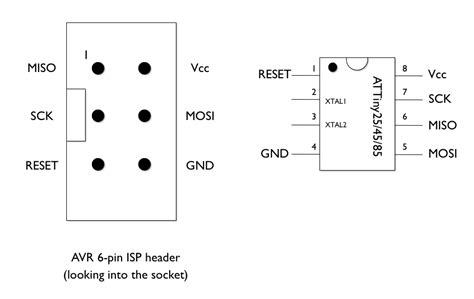
In-System Programming (ISP)
The Attiny85 supports In-System Programming (ISP), allowing you to program and reprogram the microcontroller without removing it from the circuit. This feature simplifies the development and debugging process, as you can easily update the firmware without the need for an external programmer.
Watchdog Timer
The Attiny85 includes a Watchdog Timer that can be used to detect and recover from software malfunctions. It helps ensure the reliability and stability of your projects by resetting the microcontroller if it becomes unresponsive or stuck in an infinite loop.

FAQ
-
What is the maximum operating frequency of the Attiny85?
The Attiny85 can operate at a maximum frequency of 8 MHz when powered by 2.7V to 5.5V. However, it can also operate at lower frequencies to conserve power. -
Can the Attiny85 be programmed using the Arduino IDE?
Yes, the Attiny85 can be programmed using the Arduino IDE with the help of an Arduino board acting as an ISP programmer. You need to install the necessary Attiny support files in the Arduino IDE and configure the IDE for programming the Attiny85. -
What is the flash memory size of the Attiny85?
The Attiny85 has 8 KB of flash memory for storing the program code. It also has 512 bytes of EEPROM and 512 bytes of SRAM. -
How many PWM channels does the Attiny85 have?
The Attiny85 has three PWM channels available on pins PB0, PB1, and PB4. -
Can the Attiny85 be used for battery-powered projects?
Yes, the Attiny85 is well-suited for battery-powered projects due to its low power consumption. It offers various sleep modes and power-saving features that help prolong battery life.

Conclusion
The Attiny85 is a versatile and compact microcontroller that offers a wide range of features and capabilities. Its pin configuration provides flexibility for interfacing with external components, while its low power consumption and small size make it ideal for battery-powered and space-constrained applications.
By understanding the pin functions and key features of the Attiny85, you can harness its potential and create innovative projects. Whether you’re building a small gadget, a wearable device, or an embedded system, the Attiny85 provides a reliable and efficient solution.
With its support for analog-to-digital conversion, PWM, interrupts, and various communication protocols, the Attiny85 empowers you to create interactive and intelligent projects. Its In-System Programming capability and compatibility with the Arduino IDE make it accessible to both beginners and experienced developers alike.
So, go ahead and explore the world of possibilities with the Attiny85. Let your creativity flow and bring your ideas to life using this powerful and compact microcontroller.


Leave a Reply