What is a PCBA?
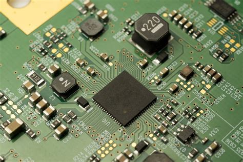
PCBA stands for Printed Circuit Board Assembly. It is a printed circuit board (PCB) that has been populated with electronic components through a series of assembly processes. The PCBA is the heart of any electronic device, connecting all the components together and allowing them to function as intended.
The Difference Between PCB and PCBA
A PCB is a bare board without any electronic components attached. It consists of a substrate made from insulating materials such as fiberglass, with conductive copper traces printed onto its surface. These traces form the electrical connections between different points on the board.
On the other hand, a PCBA is a PCB that has undergone the assembly process. Electronic components such as resistors, capacitors, integrated circuits (ICs), and connectors are soldered onto the PCB according to the design specifications. The PCBA is then ready to be installed into an electronic device.
The PCBA Assembly Process
The PCBA assembly process involves several steps, each of which must be carried out with precision and care to ensure the final product functions correctly.
Step 1: Solder Paste Application
The first step in the PCBA assembly process is to apply solder paste to the PCB. Solder paste is a mixture of tiny solder particles suspended in a flux medium. It is applied to the PCB using a stencil or screen printing process.
The stencil is a thin metal sheet with holes cut out in the shape of the pads on the PCB. The solder paste is spread over the stencil, and a squeegee is used to force the paste through the holes and onto the pads.
Step 2: Component Placement
Once the solder paste has been applied, the electronic components are placed onto the PCB. This is typically done using a pick-and-place machine, which uses vacuum nozzles to pick up the components from a tray and place them onto the PCB with high precision.
The components are placed according to the design specifications, with their leads aligned with the pads on the PCB. The solder paste holds the components in place until the soldering process is complete.
Step 3: Reflow Soldering
After the components have been placed, the PCB is passed through a reflow oven. The oven heats the PCB to a specific temperature profile, causing the solder paste to melt and form a strong bond between the component leads and the PCB pads.
The reflow soldering process is carefully controlled to ensure that the solder joints are formed correctly. The temperature profile must be followed precisely to avoid damaging the components or the PCB.
Step 4: Inspection and Testing
Once the soldering process is complete, the PCBA undergoes a series of inspections and tests to ensure that it functions correctly. This may include:
- Visual inspection: The PCBA is inspected under a microscope to check for any defects or issues with the solder joints.
- Automated optical inspection (AOI): An automated system scans the PCBA and compares it to the design specifications to check for any errors or defects.
- X-ray inspection: X-ray imaging is used to check for any hidden defects or issues with the solder joints that may not be visible on the surface.
- Functional testing: The PCBA is powered on and tested to ensure that it functions as intended.
Any issues or defects that are identified during the inspection and testing process are corrected before the PCBA is approved for use.

Types of PCBAs
There are several different types of PCBAs, each with its own unique characteristics and applications.
Single-Sided PCBAs
Single-sided PCBAs have components and copper traces on only one side of the board. They are the simplest and most cost-effective type of PCBA, but they have limitations in terms of circuit complexity and density.
Double-Sided PCBAs
Double-sided PCBAs have components and copper traces on both sides of the board. They offer more flexibility in terms of circuit design and can accommodate more components than single-sided PCBAs.
Multi-Layer PCBAs
Multi-layer PCBAs have multiple layers of copper traces separated by insulating layers. They can accommodate even more complex circuits and higher component densities than double-sided PCBAs. Multi-layer PCBAs are commonly used in advanced electronic devices such as smartphones and computers.
Flexible PCBAs
Flexible PCBAs are made from flexible materials such as polyimide, allowing them to bend and flex without breaking. They are commonly used in applications where space is limited or where the PCBA needs to conform to a specific shape.
Rigid-Flex PCBAs
Rigid-flex PCBAs combine rigid and flexible sections on the same board. The rigid sections provide structural support and can accommodate high component densities, while the flexible sections allow the PCBA to bend and flex as needed.

PCBA Design Considerations
Designing a PCBA requires careful consideration of several factors to ensure that the final product functions correctly and reliably.
Circuit Design
The first step in designing a PCBA is to create a schematic diagram of the circuit. This diagram shows the electrical connections between the components and helps to ensure that the circuit will function as intended.
The schematic diagram is then used to create a PCB layout, which shows the physical placement of the components on the board and the routing of the copper traces.
Component Selection
Selecting the right components for a PCBA is critical to ensuring its performance and reliability. Factors to consider when selecting components include:
- Electrical specifications: The components must meet the electrical requirements of the circuit, such as voltage and current ratings.
- Package size: The components must fit within the available space on the PCB.
- Thermal characteristics: The components must be able to dissipate heat effectively to avoid overheating.
- Cost: The components must be cost-effective while still meeting the performance and reliability requirements.
PCB Layout
The PCB layout is critical to the performance and reliability of the PCBA. Factors to consider when designing the PCB layout include:
- Component placement: The components must be placed in a way that minimizes the length of the copper traces and avoids interference between components.
- Trace width and spacing: The width and spacing of the copper traces must be designed to minimize resistance and crosstalk while still fitting within the available space on the PCB.
- Ground and power planes: The PCB must have adequate ground and power planes to provide a low-impedance path for current flow and to minimize noise.
- Signal integrity: The PCB layout must be designed to maintain signal integrity, particularly for high-speed signals.
Manufacturing Considerations
The design of the PCBA must also take into account the limitations and capabilities of the manufacturing process. Factors to consider include:
- Minimum feature size: The PCB layout must adhere to the minimum feature size limitations of the manufacturing process, such as the minimum trace width and spacing.
- Soldermask and silkscreen: The soldermask and silkscreen layers must be designed to provide adequate insulation and labeling while still allowing for proper soldering.
- Panelization: The PCB layout must be designed to allow for efficient panelization, which involves grouping multiple PCBs together on a single panel for manufacturing.

PCBA Testing and Quality Control
Ensuring the quality and reliability of PCBAs requires rigorous testing and quality control measures throughout the manufacturing process.
In-Circuit Testing (ICT)
In-circuit testing involves using a special test fixture to make electrical contact with each component on the PCBA and testing its functionality. ICT can detect issues such as missing or incorrect components, short circuits, and open circuits.
Flying Probe Testing
Flying probe testing uses a set of movable probes to make contact with specific points on the PCBA and test their electrical characteristics. Flying probe testing is slower than ICT but can be used for low-volume production or prototypes.
Boundary Scan Testing
Boundary scan testing uses a special test access port (TAP) built into the components on the PCBA to test their functionality and interconnections. Boundary scan testing can detect issues such as open or short circuits and can be used to program devices such as FPGAs and microcontrollers.
Functional Testing
Functional testing involves powering on the PCBA and testing its functionality under real-world conditions. Functional testing can detect issues such as incorrect component values, timing problems, and software bugs.
Environmental Testing
Environmental testing involves subjecting the PCBA to various environmental stresses such as temperature, humidity, and vibration to ensure that it can withstand the conditions it will encounter in use. Environmental testing can help to identify design or manufacturing issues that may not be apparent under normal conditions.
PCBA Quality Standards
There are several industry standards that govern the quality and reliability of PCBAs. Some of the most common standards include:
- IPC-A-610: Acceptability of Electronic Assemblies
- IPC-J-STD-001: Requirements for Soldered Electrical and Electronic Assemblies
- IPC-6012: Qualification and Performance Specification for Rigid Printed Boards
- IPC-6013: Qualification and Performance Specification for Flexible/Rigid-Flexible Printed Boards
These standards provide guidance on factors such as component placement, soldering, and inspection criteria to ensure that PCBAs meet the required level of quality and reliability.
Advantages of PCBAs
PCBAs offer several advantages over other types of electronic assemblies, such as point-to-point wiring or wire wrapping.
Compact Size
PCBAs allow for a much higher component density than other types of assemblies, enabling the creation of smaller and more compact electronic devices.
Reliability
PCBAs are highly reliable due to the use of automated manufacturing processes and rigorous quality control measures. The solid copper traces on the PCB provide a low-resistance path for current flow, and the solder joints between the components and the PCB are strong and durable.
Consistency
PCBAs are manufactured using automated processes, which ensures a high degree of consistency between units. This consistency is critical for electronic devices that require precise and repeatable performance.
Cost-Effective
PCBAs are cost-effective for high-volume production due to the use of automated manufacturing processes. The cost per unit decreases as the volume increases, making PCBAs an attractive option for mass-produced electronic devices.
Applications of PCBAs
PCBAs are used in a wide range of electronic devices, from consumer electronics to industrial equipment. Some common applications include:
- Smartphones and tablets
- Computers and laptops
- Televisions and audio equipment
- Automotive electronics
- Medical devices
- Industrial control systems
- Aerospace and defense electronics
Future Trends in PCBA Technology
As electronic devices continue to become smaller, more powerful, and more complex, PCBA technology must evolve to keep pace. Some of the key trends in PCBA technology include:
Miniaturization
The demand for smaller and more compact electronic devices is driving the development of newer technologies such as chip-on-board (COB) and chip-scale packaging (CSP), which allow for even higher component densities than traditional PCBAs.
High-Speed Design
The increasing speed and complexity of electronic devices require PCBAs that can support high-speed signals without interference or distortion. Newer PCB materials and design techniques are being developed to meet these challenges.
3D Printing
3D printing technology is being explored as a way to create PCBAs with complex geometries and embedded components. This could enable the creation of highly customized and integrated electronic devices.
Sustainability
There is a growing focus on sustainability in the electronics industry, and PCBAs are no exception. Newer materials and manufacturing processes are being developed to reduce the environmental impact of PCBAs, such as the use of lead-free solder and recyclable PCB substrates.
Frequently Asked Questions (FAQ)
What is the difference between a PCB and a PCBA?
A PCB is a bare board without any electronic components attached, while a PCBA is a PCB that has undergone the assembly process and has electronic components soldered onto it.
What are the steps in the PCBA assembly process?
The main steps in the PCBA assembly process are:
1. Solder paste application
2. Component placement
3. Reflow soldering
4. Inspection and testing
What are some common types of PCBAs?
Some common types of PCBAs include:
– Single-sided PCBAs
– Double-sided PCBAs
– Multi-layer PCBAs
– Flexible PCBAs
– Rigid-flex PCBAs
What are some key considerations when designing a PCBA?
Some key considerations when designing a PCBA include:
– Circuit design
– Component selection
– PCB layout
– Manufacturing considerations
What are some common testing methods used for PCBAs?
Some common testing methods used for PCBAs include:
– In-circuit testing (ICT)
– Flying probe testing
– Boundary scan testing
– Functional testing
– Environmental testing
Conclusion
PCBAs are the backbone of modern electronic devices, providing the electrical connections and functionality that make these devices possible. The PCBA assembly process involves a series of precise and automated steps to ensure that the final product meets the required level of quality and reliability.
Designing and manufacturing PCBAs requires careful consideration of factors such as circuit design, component selection, PCB layout, and manufacturing processes. Rigorous testing and quality control measures are also critical to ensuring the performance and reliability of PCBAs.
As electronic devices continue to evolve and become more complex, PCBA technology must also evolve to keep pace. Trends such as miniaturization, high-speed design, 3D printing, and sustainability are shaping the future of PCBA technology and the electronics industry as a whole.


Leave a Reply