Introduction to PCB Antennas
Printed Circuit Board (PCB) antennas have become increasingly popular in modern wireless communication devices due to their compact size, low cost, and ease of integration. These antennas are designed and fabricated directly onto the PCB, eliminating the need for external antennas and reducing the overall size of the device. PCB antennas are widely used in various applications, such as smartphones, tablets, laptops, and Internet of Things (IoT) devices, for receiving and transmitting wireless signals.
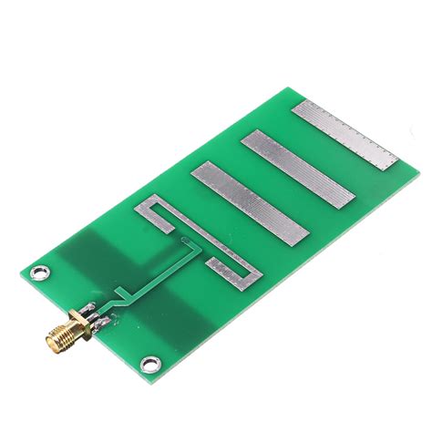
Types of PCB Antennas
There are several types of PCB antennas, each with its own characteristics and advantages:
-
Microstrip Antennas: Also known as patch antennas, these are the most common type of PCB antennas. They consist of a metallic patch printed on one side of the PCB, with a ground plane on the other side. Microstrip antennas are simple to design and fabricate, and they offer moderate gain and bandwidth.
-
Dipole Antennas: Dipole antennas are composed of two equal-length conductive elements, such as copper traces, printed on the PCB. They are easy to design and provide omnidirectional radiation patterns, making them suitable for applications that require coverage in all directions.
-
Inverted-F Antennas (IFA): IFA antennas are a variant of monopole antennas that are folded to reduce their size. They are compact and have a low profile, making them ideal for small wireless devices. IFA antennas offer good performance in terms of gain and bandwidth.
-
Loop Antennas: Loop antennas are formed by printing a circular or rectangular loop of conductive material on the PCB. They are compact and provide a omnidirectional radiation pattern. Loop antennas are often used in near-field communication (NFC) applications.
-
Vivaldi Antennas: Vivaldi antennas, also known as tapered slot antennas, are wideband antennas that offer high gain and directivity. They are designed by etching a tapered slot on the PCB, which gradually widens towards the antenna’s aperture. Vivaldi antennas are commonly used in ultra-wideband (UWB) applications.
Design Considerations for PCB Antennas
When designing PCB antennas, several factors must be taken into account to ensure optimal performance:
Frequency and Bandwidth
The operating frequency and bandwidth of the antenna are critical factors in the design process. The antenna’s dimensions, such as the patch size or dipole length, must be calculated based on the desired frequency. The bandwidth of the antenna determines the range of frequencies over which it can operate effectively.
Substrate Material and Thickness
The choice of substrate material and its thickness significantly impact the antenna’s performance. The substrate’s dielectric constant and loss tangent affect the antenna’s efficiency, bandwidth, and radiation characteristics. Common substrate materials for PCB antennas include FR-4, Rogers, and Taconic.
Ground Plane and Feeding Techniques
The ground plane plays a crucial role in the antenna’s performance, as it affects the radiation pattern and impedance matching. The size and shape of the ground plane must be carefully designed to achieve the desired characteristics. The feeding technique, such as microstrip line, coaxial probe, or aperture coupling, also influences the antenna’s performance and should be selected based on the specific application requirements.
Antenna Placement and Integration
The placement of the antenna on the PCB is critical to ensure optimal performance and minimize interference with other components. The antenna should be located away from noise sources, such as digital circuits or power lines, to reduce electromagnetic interference (EMI). Proper integration of the antenna with the PCB layout and other components is essential for achieving the desired performance.

Simulation and Optimization
To ensure the desired performance of PCB antennas, simulation and optimization tools are widely used in the design process. These tools allow engineers to model and analyze the antenna’s behavior before fabrication, reducing the time and cost associated with physical prototyping.
Electromagnetic Simulation Software
Electromagnetic (EM) simulation software, such as Ansys HFSS, CST Studio Suite, or Altair Feko, enables the accurate modeling and simulation of PCB antennas. These tools solve Maxwell’s equations numerically to predict the antenna’s radiation characteristics, impedance matching, and overall performance. EM simulation helps in identifying potential issues and optimizing the antenna design before fabrication.
Optimization Techniques
Optimization techniques are employed to fine-tune the antenna’s performance based on the specified design goals. These techniques involve iteratively adjusting the antenna’s parameters, such as dimensions, substrate properties, or feeding configurations, to achieve the desired characteristics. Optimization algorithms, such as genetic algorithms or particle swarm optimization, are commonly used in conjunction with EM simulation software to automate the optimization process.

Fabrication and Testing
Once the PCB antenna design is finalized and optimized through simulation, the next step is fabrication and testing.
PCB Fabrication Process
The fabrication of PCB antennas involves the same process as regular PCBs. The designed antenna layout is converted into Gerber files, which are used by PCB manufacturers to create the physical board. The fabrication process includes etching the copper traces, applying solder mask, and adding silkscreen labels. Special attention must be given to the tolerances and quality control during the fabrication process to ensure the antenna’s performance matches the simulated results.
Antenna Measurement and Testing
After fabrication, the PCB antenna must undergo rigorous testing to validate its performance. Antenna measurement techniques, such as far-field or near-field measurements, are used to characterize the antenna’s radiation pattern, gain, efficiency, and impedance matching. These measurements are typically conducted in an anechoic chamber to minimize external interference and reflections. The measured results are compared with the simulated data to ensure the antenna meets the design specifications.

Applications of PCB Antennas
PCB antennas find applications in a wide range of wireless communication devices and systems:
Wireless Communication Devices
PCB antennas are extensively used in smartphones, tablets, laptops, and other portable devices for wireless connectivity. These antennas enable communication through various wireless standards, such as Wi-Fi, Bluetooth, GPS, and cellular networks (e.g., 4G LTE, 5G). The compact size and low profile of PCB antennas make them ideal for integration into these devices.
Internet of Things (IoT) Devices
IoT devices, such as smart home appliances, wearables, and industrial sensors, rely on PCB antennas for wireless communication. These antennas enable the devices to connect to the internet and communicate with other devices or cloud platforms. PCB antennas designed for IoT applications must be optimized for low power consumption and long-range communication.
Automotive and Transportation Systems
PCB antennas are employed in various automotive and transportation applications, such as vehicle-to-vehicle (V2V) communication, vehicle-to-infrastructure (V2I) communication, and GPS navigation. These antennas enable the exchange of critical information between vehicles and infrastructure, enhancing safety and efficiency. PCB antennas used in automotive applications must be designed to withstand harsh environmental conditions and meet stringent reliability requirements.
Medical Devices
PCB antennas are used in medical devices for wireless monitoring and communication. Applications include wearable health monitors, implantable devices, and remote patient monitoring systems. PCB antennas in medical devices must be designed to ensure reliable and secure data transmission while complying with regulatory standards for electromagnetic compatibility (EMC) and specific absorption rate (SAR) limits.
Future Trends and Challenges
The field of PCB antennas continues to evolve, driven by the increasing demand for high-speed wireless communication, miniaturization, and the emergence of new technologies.
5G and Beyond
The deployment of 5G networks and the development of future wireless technologies (e.g., 6G) present new challenges and opportunities for PCB antenna design. These networks operate at higher frequencies, such as millimeter-wave (mmWave) bands, requiring the design of compact, high-gain, and wideband antennas. PCB antennas for 5G and beyond must also support advanced techniques, such as massive MIMO and beamforming, to enhance capacity and coverage.
Antenna Miniaturization
The trend towards miniaturization of wireless devices demands the development of even smaller and more compact PCB antennas. Novel antenna designs, such as fractal antennas or metamaterial-based antennas, are being explored to achieve miniaturization without compromising performance. Advanced manufacturing techniques, such as 3D printing or inkjet printing, are also being investigated for the fabrication of compact and flexible PCB antennas.
Integration with Advanced Materials
The integration of PCB antennas with advanced materials, such as graphene or conductive polymers, offers new possibilities for enhancing antenna performance. These materials exhibit unique electrical and mechanical properties that can improve the antenna’s efficiency, bandwidth, and flexibility. Research is ongoing to develop innovative PCB antenna designs that leverage the benefits of these advanced materials.
Energy Harvesting and Wireless Power Transfer
PCB antennas are also being explored for energy harvesting and wireless power transfer applications. By designing antennas that can efficiently capture ambient electromagnetic energy, such as RF signals or solar radiation, it is possible to power small electronic devices without the need for batteries. PCB antennas can also be used for near-field wireless power transfer, enabling the charging of devices over short distances.
Frequently Asked Questions (FAQ)
-
What is a PCB antenna?
A PCB antenna is an antenna that is designed and fabricated directly onto a printed circuit board (PCB). It is a compact and cost-effective solution for wireless communication devices. -
What are the advantages of using PCB antennas?
PCB antennas offer several advantages, including compact size, low cost, ease of integration, and the ability to be customized for specific applications. They eliminate the need for external antennas, reducing the overall size of the device. -
What factors should be considered when designing a PCB antenna?
When designing a PCB antenna, key factors to consider include the operating frequency and bandwidth, substrate material and thickness, ground plane and feeding techniques, and antenna placement and integration. These factors influence the antenna’s performance and must be carefully optimized. -
How are PCB antennas simulated and optimized?
PCB antennas are simulated and optimized using electromagnetic (EM) simulation software, such as Ansys HFSS, CST Studio Suite, or Altair Feko. These tools enable the accurate modeling and analysis of the antenna’s performance before fabrication. Optimization techniques, such as genetic algorithms or particle swarm optimization, are used to fine-tune the antenna’s parameters to achieve the desired characteristics. -
What are some common applications of PCB antennas?
PCB antennas find applications in a wide range of wireless communication devices and systems, including smartphones, tablets, laptops, IoT devices, automotive and transportation systems, and medical devices. They enable wireless connectivity through various standards, such as Wi-Fi, Bluetooth, GPS, and cellular networks.
Conclusion
PCB antennas have revolutionized the field of wireless communication by providing a compact, cost-effective, and easily integrable solution for receiving and transmitting signals. These antennas are designed and fabricated directly onto the PCB, offering several advantages over traditional external antennas. The design of PCB antennas involves careful consideration of various factors, such as frequency, bandwidth, substrate properties, ground plane, and feeding techniques. Simulation and optimization tools play a crucial role in ensuring the desired performance of PCB antennas before fabrication.
PCB antennas find extensive applications in wireless communication devices, IoT systems, automotive and transportation, and medical devices. As wireless technologies continue to evolve, PCB antennas face new challenges and opportunities, such as the demand for higher frequencies, miniaturization, integration with advanced materials, and energy harvesting capabilities. Ongoing research and development in the field of PCB antennas aim to address these challenges and enable the next generation of wireless communication systems.


Leave a Reply