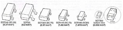
What are SMD Packages?
Surface-mount device (SMD) packages are a type of packaging for electronic components that are designed to be mounted directly onto the surface of a printed circuit board (PCB). SMD packages have largely replaced through-hole mounting in most applications due to their smaller size, lower cost, and better high-frequency performance.
SMD packages come in a wide variety of shapes and sizes, each with their own advantages and disadvantages. Some of the most common types of SMD packages include:
- Chip packages (e.g. 0201, 0402, 0603, 0805, 1206)
- Small Outline Integrated Circuit (SOIC)
- Quad Flat Package (QFP)
- Ball Grid Array (BGA)
- Quad Flat No-Lead (QFN)
- Land Grid Array (LGA)
In this article, we will explore each of these SMD package types in more detail, including their characteristics, applications, and design considerations.
Chip Packages
Chip packages, also known as chip resistors or chip capacitors, are the smallest and simplest type of SMD package. They consist of a small rectangular block of ceramic or plastic with metallized end caps that serve as the electrical terminals.
Chip packages are identified by a 4-digit code that specifies their dimensions in hundredths of an inch. For example, an 0402 package measures 0.04 inches by 0.02 inches (1.0mm x 0.5mm), while a 1206 package measures 0.12 inches by 0.06 inches (3.2mm x 1.6mm).
The most common chip package sizes and their dimensions are shown in the table below:
| Package Size | Dimensions (Imperial) | Dimensions (Metric) |
|---|---|---|
| 01005 | 0.016″ x 0.008″ | 0.4mm x 0.2mm |
| 0201 | 0.024″ x 0.012″ | 0.6mm x 0.3mm |
| 0402 | 0.040″ x 0.020″ | 1.0mm x 0.5mm |
| 0603 | 0.063″ x 0.031″ | 1.6mm x 0.8mm |
| 0805 | 0.080″ x 0.050″ | 2.0mm x 1.25mm |
| 1206 | 0.126″ x 0.063″ | 3.2mm x 1.6mm |
| 1210 | 0.126″ x 0.100″ | 3.2mm x 2.5mm |
| 1812 | 0.18″ x 0.12″ | 4.5mm x 3.2mm |
| 2010 | 0.20″ x 0.10″ | 5.0mm x 2.5mm |
| 2512 | 0.25″ x 0.12″ | 6.3mm x 3.2mm |
Chip packages are commonly used for passive components such as resistors, capacitors, and inductors. They are also used for some active components such as diodes, transistors, and integrated circuits.
The main advantages of chip packages are their small size, low cost, and ease of assembly. They can be easily placed and soldered onto a PCB using automated pick-and-place machines and reflow soldering processes.
However, chip packages also have some limitations. Their small size can make them difficult to handle and inspect, and they may be prone to tombstoning (lifting up on one end) during soldering. They also have limited power handling capability and may not be suitable for high-power applications.

Small Outline Integrated Circuit (SOIC)
The Small Outline Integrated Circuit (SOIC) is a type of surface-mount package that is commonly used for analog and digital integrated circuits. It consists of a rectangular plastic or ceramic body with two rows of leads extending from the sides.
SOIC packages are identified by the number of leads and the lead pitch (spacing between leads). The most common SOIC packages are:
- SOIC-8: 8 leads, 1.27mm pitch
- SOIC-14: 14 leads, 1.27mm pitch
- SOIC-16: 16 leads, 1.27mm pitch
- SOIC-20: 20 leads, 1.27mm pitch
- SOIC-24: 24 leads, 1.27mm pitch
- SOIC-28: 28 leads, 1.27mm pitch
The dimensions of SOIC packages vary depending on the number of leads, but they typically range from 4mm to 15mm in length and 3.9mm to 10.3mm in width. The height is usually around 2mm.
SOIC packages offer several advantages over chip packages for integrated circuits:
- They have more leads, allowing for more complex circuits and higher pin counts
- The leads are spaced farther apart, making them easier to solder and inspect
- They have higher power dissipation capability due to the larger package size
- They provide better mechanical protection for the IC die
However, SOIC packages are larger and more expensive than chip packages, and they require more board space. They also have higher parasitic inductance and capacitance due to the longer leads, which can affect high-frequency performance.

Quad Flat Package (QFP)
The Quad Flat Package (QFP) is another common SMD package for integrated circuits. It is similar to the SOIC package, but has leads on all four sides of the package instead of just two.
QFP packages are identified by the number of leads and the lead pitch, as well as the package size. The most common QFP packages are:
- TQFP (Thin QFP): 32 to 176 leads, 0.5mm to 0.8mm pitch, 5mm to 14mm square
- LQFP (Low-profile QFP): 32 to 100 leads, 0.5mm to 0.65mm pitch, 5mm to 10mm square
- PQFP (Plastic QFP): 44 to 256 leads, 0.4mm to 0.8mm pitch, 10mm to 28mm square
- CQFP (Ceramic QFP): 84 to 256 leads, 0.5mm to 0.8mm pitch, 20mm to 40mm square
The main advantage of QFP packages over SOIC packages is the higher pin count, which allows for more complex circuits and higher levels of integration. QFP packages also have better thermal dissipation due to the larger package size and the presence of a thermal pad on the bottom of the package.
However, QFP packages are larger and more expensive than SOIC packages, and they require more board space. They also have higher lead inductance and capacitance, which can affect signal integrity and high-frequency performance.

Ball Grid Array (BGA)
The Ball Grid Array (BGA) is a type of SMD package that uses an array of solder balls on the bottom of the package to provide electrical connectivity to the PCB. BGA packages are commonly used for high-density, high-performance integrated circuits such as microprocessors, FPGAs, and ASICs.
BGA packages are identified by the number and arrangement of the solder balls, as well as the package size. The most common types of BGA packages are:
- PBGA (Plastic BGA): Plastic substrate, wire-bonded die, 0.5mm to 1.27mm ball pitch, 5mm to 27mm square
- CBGA (Ceramic BGA): Ceramic substrate, wire-bonded die, 1.27mm ball pitch, 15mm to 50mm square
- TBGA (Tape BGA): Polyimide tape substrate, wire-bonded or flip-chip die, 0.5mm to 0.8mm ball pitch, 5mm to 15mm square
- FBGA (Fine-pitch BGA): Plastic or ceramic substrate, wire-bonded or flip-chip die, 0.3mm to 0.5mm ball pitch, 5mm to 15mm square
BGA packages offer several advantages over other SMD packages:
- Higher pin density due to the use of an area array instead of peripheral leads
- Better thermal and electrical performance due to the shorter paths between the die and the PCB
- Smaller package size and lighter weight compared to QFP packages with the same pin count
- Better solder joint reliability due to the use of solder balls instead of leads
However, BGA packages also have some disadvantages:
- Higher cost due to the more complex manufacturing process and materials
- More difficult to inspect and rework due to the hidden solder joints under the package
- Requires more precise placement and soldering equipment due to the smaller pitch and higher pin count
- May require additional PCB layers and vias to route the high-density interconnects
Quad Flat No-Lead (QFN)
The Quad Flat No-Lead (QFN) package, also known as a Micro Lead Frame (MLF) package, is a type of SMD package that has a small footprint and a low profile. It is similar to a QFP package, but has no leads extending from the sides of the package. Instead, the electrical contacts are located on the bottom of the package in the form of exposed copper pads.
QFN packages are identified by the number of pins and the package size. The most common QFN packages are:
- QFN-16: 16 pins, 3mm x 3mm
- QFN-24: 24 pins, 4mm x 4mm
- QFN-32: 32 pins, 5mm x 5mm
- QFN-48: 48 pins, 7mm x 7mm
QFN packages offer several advantages over other SMD packages:
- Smaller footprint and lower profile compared to QFP packages with the same pin count
- Better thermal performance due to the exposed copper pad on the bottom of the package
- Lower lead inductance and capacitance due to the shorter paths between the die and the PCB
- Lower cost compared to BGA packages with the same pin count
However, QFN packages also have some disadvantages:
- More difficult to inspect and rework due to the hidden solder joints under the package
- Requires more precise placement and soldering equipment due to the smaller pitch and lack of leads
- May require additional thermal vias and heatsinks to dissipate heat from the exposed copper pad
- Limited pin count compared to BGA packages
Land Grid Array (LGA)
The Land Grid Array (LGA) package is a type of SMD package that is similar to a BGA package, but uses a grid of flat contact pads instead of solder balls. LGA packages are commonly used for high-density, high-performance integrated circuits that require low-profile and low-inductance interconnects.
LGA packages are identified by the number and arrangement of the contact pads, as well as the package size. The most common types of LGA packages are:
- LGA-775: 775 contacts, 37.5mm x 37.5mm, 1.27mm pitch, used for Intel desktop processors
- LGA-1156: 1156 contacts, 40mm x 40mm, 1.0mm pitch, used for Intel desktop processors
- LGA-1366: 1366 contacts, 45mm x 45mm, 1.0mm pitch, used for Intel high-end desktop and server processors
- LGA-2011: 2011 contacts, 52.5mm x 45mm, 1.0mm pitch, used for Intel high-end desktop and server processors
LGA packages offer several advantages over BGA packages:
- Lower cost due to the simpler manufacturing process and materials
- Better thermal performance due to the larger contact area between the package and the PCB
- Lower profile and lighter weight due to the lack of solder balls
- Easier to inspect and rework due to the exposed contact pads
However, LGA packages also have some disadvantages:
- Requires a clamping mechanism to maintain contact between the package and the PCB
- May require a custom socket or interposer to provide electrical connectivity
- Higher insertion force and potential for damage during assembly and disassembly
- Limited pin count compared to BGA packages with the same footprint
FAQ
1. What are the advantages of using SMD packages over through-hole packages?
SMD packages offer several advantages over through-hole packages:
- Smaller size and lighter weight, allowing for higher component density and smaller PCBs
- Lower cost due to the simpler manufacturing process and materials
- Better high-frequency performance due to the shorter lead lengths and lower parasitic inductance and capacitance
- Easier to assemble using automated pick-and-place machines and reflow soldering processes
2. What are the most common types of SMD packages?
The most common types of SMD packages are:
- Chip packages (e.g. 0201, 0402, 0603, 0805, 1206) for passive components
- Small Outline Integrated Circuit (SOIC) for analog and digital ICs
- Quad Flat Package (QFP) for high-pin-count ICs
- Ball Grid Array (BGA) for high-density, high-performance ICs
- Quad Flat No-Lead (QFN) for low-profile, low-cost ICs
- Land Grid Array (LGA) for high-density, high-performance ICs with low-profile and low-inductance requirements
3. How do I choose the right SMD package for my component?
Choosing the right SMD package for your component depends on several factors:
- The type and function of the component (e.g. passive, analog, digital, high-speed, high-power)
- The number of pins or terminals required
- The size and weight constraints of the PCB
- The thermal and electrical performance requirements
- The cost and availability of the package and the associated assembly processes
In general, smaller packages like chip packages and QFN are preferred for low-pin-count, low-power components, while larger packages like QFP and BGA are used for high-pin-count, high-performance components. SOIC and LGA packages offer a balance of size, performance, and cost for many applications.
4. What are the challenges of working with SMD packages?
Working with SMD packages presents several challenges compared to through-hole packages:
- Smaller size and pitch, requiring more precise placement and soldering equipment
- Hidden solder joints under the package, making inspection and rework more difficult
- Potential for tombstoning, bridging, and other soldering defects due to the smaller size and closer spacing of the leads or pads
- Higher thermal and mechanical stress on the PCB and components due to the smaller size and lower standoff height
- Need for specialized handling and storage equipment to prevent damage from electrostatic discharge (ESD) and moisture
To overcome these challenges, designers and manufacturers need to follow best practices for SMD package selection, PCB layout, assembly process control, and quality assurance.
5. What are the future trends in SMD packaging?
The future trends in SMD packaging are driven by the increasing demand for smaller, faster, and more integrated electronic devices. Some of the key trends include:
- Smaller and thinner packages with higher pin density and lower profile, such as chip-scale packages (CSP) and wafer-level packages (WLP)
- Advanced packaging technologies such as 2.5D and 3D integration, using through-silicon vias (TSVs) and interposers to stack multiple dies and packages
- Increased use of embedded components and passive integration to reduce PCB size and improve performance
- Adoption of lead-free and halogen-free materials to meet environmental and regulatory requirements
- Development of new materials and processes for high-frequency, high-power, and harsh-environment applications, such as gallium nitride (GaN) and silicon carbide (SiC) devices
As electronic devices continue to evolve and new applications emerge, SMD packaging will remain a critical enabler of innovation and performance in the electronics industry.


Leave a Reply