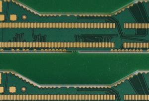
Introduction to Immersion Gold PCB Plating
Immersion gold (ENIG) plating is a popular surface finish for printed circuit boards (PCBs) due to its numerous benefits. This chemical process deposits a thin layer of gold over a nickel layer on the copper pads and through-holes of the PCB. The resulting finish offers excellent solderability, durability, and reliability, making it a preferred choice for many electronic applications.
In this article, we will explore the 13 key advantages of immersion gold PCB plating and why it has become a go-to choice for PCB manufacturers and designers.
Advantage 1: Excellent Solderability
One of the primary advantages of immersion gold plating is its exceptional solderability. The gold layer provides a clean, oxide-free surface that allows for easy and reliable soldering of components. This is particularly important for surface mount technology (SMT) components, which require precise and consistent solder joints.
The solderability of immersion gold is superior to other surface finishes, such as organic solderability preservatives (OSP) and hot air solder leveling (HASL). The gold layer remains solderable even after extended storage periods, ensuring that the PCBs can be assembled efficiently and with minimal issues.

Advantage 2: Long Shelf Life
Another significant benefit of immersion gold plating is its long shelf life. PCBs with an immersion gold finish can be stored for extended periods without compromising their solderability or functionality. This is because the gold layer acts as a protective barrier, preventing the oxidation and contamination of the underlying copper and nickel layers.
The long shelf life of immersion gold-plated PCBs is particularly valuable for manufacturers who produce boards in large quantities or for customers who require a long lead time between PCB fabrication and assembly. It also reduces the need for expensive nitrogen storage or other preservation methods.

Advantage 3: Durability and Wear Resistance
Immersion gold plating provides excellent durability and wear resistance to PCBs. The gold layer is highly resistant to corrosion, abrasion, and other forms of physical damage. This makes immersion gold-plated PCBs suitable for use in harsh environments or applications where the boards are subject to frequent handling or exposure to chemicals.
The durability of immersion gold also extends to the solder joints. The gold layer helps to prevent solder joint fatigue and cracking, which can occur due to thermal cycling or mechanical stress. This enhances the overall reliability and longevity of the assembled PCBs.

Advantage 4: Compatibility with Fine-Pitch Components
Immersion gold plating is particularly advantageous for PCBs with fine-pitch components, such as ball grid arrays (BGAs) and quad-flat no-leads (QFNs). The thin and uniform gold layer allows for precise and reliable soldering of these components, ensuring proper electrical connections and minimizing the risk of bridging or shorts.
The compatibility of immersion gold with fine-pitch components is essential for modern electronics, where device miniaturization and high-density packaging are increasingly common. It enables designers to create compact and high-performance PCBs without compromising on manufacturability or reliability.
Advantage 5: Excellent Electrical Performance
Immersion gold plating offers excellent electrical performance, making it suitable for high-frequency and high-speed applications. The gold layer provides a low-resistance and low-inductance path for electrical signals, minimizing signal loss and distortion.
Moreover, the nickel layer beneath the gold acts as a diffusion barrier, preventing the formation of intermetallic compounds between the gold and copper layers. This helps to maintain the integrity of the electrical connections and prevent signal degradation over time.
Advantage 6: RoHS Compliance
Immersion gold plating is compliant with the Restriction of Hazardous Substances (RoHS) directive, which limits the use of certain hazardous materials in electronic products. Unlike some other surface finishes, such as lead-based HASL, immersion gold does not contain any restricted substances.
RoHS compliance is a legal requirement for electronic products sold in many countries, including the European Union. By using immersion gold plating, PCB manufacturers can ensure that their boards meet these regulatory standards and can be used in a wide range of applications.
Advantage 7: Compatibility with Various Solderable Finishes
Immersion gold plating is compatible with a variety of solderable finishes, including lead-free solders and tin-lead solders. This versatility allows PCB manufacturers to use immersion gold in conjunction with other surface finishes, depending on the specific requirements of the application.
For example, a PCB may have immersion gold plating on the component pads and HASL or OSP on the edge connectors. This hybrid approach can provide the benefits of immersion gold where it is most needed while using a more cost-effective finish on other areas of the board.
Advantage 8: Ease of Inspection
Immersion gold-plated PCBs are easy to inspect visually, as the gold layer provides a clear and distinct contrast against the PCB substrate. This makes it easier for quality control personnel to identify any defects or irregularities in the surface finish, such as voids, nodules, or contamination.
The ease of inspection is particularly important for high-reliability applications, where even minor defects can have serious consequences. It also helps to streamline the PCB manufacturing process, reducing the time and cost associated with quality control.
Advantage 9: Improved Coplanarity
Immersion gold plating helps to improve the coplanarity of PCBs, which is the degree to which the surfaces of the component pads are level and parallel to each other. Good coplanarity is essential for the proper seating and soldering of surface mount components, particularly those with fine pitch or low clearance.
The thin and uniform gold layer provided by immersion gold plating helps to minimize any variations in the surface height of the component pads. This, in turn, ensures better coplanarity and reduces the risk of component misalignment or poor solder joints.
Advantage 10: Compatibility with Wire Bonding
Immersion gold plating is compatible with wire bonding, a process used to make electrical connections between semiconductor chips and PCBs. The gold layer provides an ideal surface for wire bonding, as it is soft, ductile, and has excellent adhesion properties.
Wire bonding is commonly used in high-reliability applications, such as aerospace, defense, and medical electronics. The compatibility of immersion gold with wire bonding makes it a preferred choice for these industries, where the integrity and reliability of the electrical connections are of utmost importance.
Advantage 11: Aesthetics and Branding
Immersion gold-plated PCBs have an attractive and professional appearance, with a bright and shiny gold finish. This aesthetic appeal can be important for certain applications, such as consumer electronics or luxury products, where the visual quality of the PCB is a key consideration.
Moreover, the gold finish can be used for branding purposes, as it allows for the inclusion of logos, text, or other graphics on the PCB surface. This can help to enhance the brand image and create a more memorable product experience for the end-user.
Advantage 12: Cost-Effectiveness
Although immersion gold plating is generally more expensive than some other surface finishes, such as OSP or HASL, it can be a cost-effective choice in the long run. The superior solderability, durability, and reliability of immersion gold can help to reduce the overall cost of PCB assembly and rework.
Furthermore, the long shelf life of immersion gold-plated PCBs can help to minimize the cost of inventory management and storage. This is particularly relevant for manufacturers who produce boards in large quantities or for customers who require a long lead time between PCB fabrication and assembly.
Advantage 13: Suitability for High-Reliability Applications
Immersion gold plating is an excellent choice for high-reliability applications, such as aerospace, defense, medical, and automotive electronics. The numerous benefits of immersion gold, including its solderability, durability, and compatibility with fine-pitch components and wire bonding, make it well-suited for these demanding environments.
In high-reliability applications, the cost of PCB failure can be extremely high, both in terms of financial losses and potential safety risks. By using immersion gold plating, manufacturers can ensure that their PCBs meet the stringent reliability and performance requirements of these industries.
Immersion Gold PCB Plating Comparison Table
| Surface Finish | Solderability | Shelf Life | Durability | Fine-Pitch Compatibility | RoHS Compliance |
|---|---|---|---|---|---|
| Immersion Gold | Excellent | Long | High | Excellent | Yes |
| HASL | Good | Moderate | Moderate | Limited | No (Lead-based) |
| OSP | Moderate | Short | Low | Good | Yes |
| ENEPIG | Excellent | Long | High | Excellent | Yes |
Frequently Asked Questions (FAQ)
1. What is the typical thickness of the gold layer in immersion gold plating?
The typical thickness of the gold layer in immersion gold plating ranges from 0.05 to 0.2 micrometers (2 to 8 microinches). The exact thickness depends on the specific requirements of the application and the PCB manufacturer’s process.
2. Can immersion gold-plated PCBs be reworked or repaired?
Yes, immersion gold-plated PCBs can be reworked or repaired, although the process may be more challenging than with other surface finishes. The gold layer must be removed from the area to be reworked, typically using a solder wick or a specialized desoldering tool. After the repair is complete, the gold layer can be reapplied using a selective plating process.
3. How does the cost of immersion gold compare to other surface finishes?
Immersion gold plating is generally more expensive than OSP and HASL, but less expensive than ENEPIG (electroless nickel / electroless palladium / immersion gold). However, the exact cost difference depends on various factors, such as the PCB design, the manufacturing volume, and the specific process used by the PCB manufacturer.
4. Can immersion gold plating be used on flexible PCBs?
Yes, immersion gold plating can be used on flexible PCBs, although the process may require some modifications to account for the different material properties and handling requirements of flexible substrates. The gold layer can help to improve the durability and reliability of the flexible PCB, especially in applications where the board is subject to repeated bending or flexing.
5. How does immersion gold plating differ from ENEPIG?
Immersion gold plating and ENEPIG (electroless nickel / electroless palladium / immersion gold) are similar surface finishes, but with some key differences. ENEPIG includes an additional layer of palladium between the nickel and gold layers, which provides even better solderability and durability than immersion gold alone. However, ENEPIG is also more expensive and may require a more complex manufacturing process.
Conclusion
Immersion gold plating offers a wide range of advantages for PCBs, making it a popular choice for many electronic applications. Its excellent solderability, long shelf life, durability, and compatibility with fine-pitch components and wire bonding make it well-suited for high-reliability industries, such as aerospace, defense, and medical electronics.
Although immersion gold may have a higher initial cost than some other surface finishes, its superior performance and reliability can make it a cost-effective choice in the long run. As PCB designs continue to become more complex and demanding, the benefits of immersion gold plating will likely make it an increasingly important tool for PCB manufacturers and designers.


Leave a Reply