Introduction
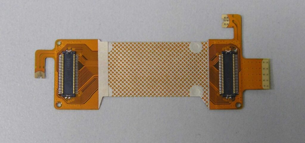
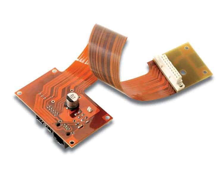
Flexible printed circuit boards (FPCs) play an integral role in modern electronics by enabling connection between components in tight spaces. FPCs are made from flexible insulating material with conductive traces etched or printed on them. Unlike rigid PCBs, FPCs can bend and twist to accommodate three-dimensional configurations.
FPCs provide several benefits:
- Compact size – FPCs can fit into tight spaces and move dynamically. This is critical for compact devices like wearables and medical devices.
- Durability – Flex circuits can withstand vibration, shock, and repeated bending. This makes them well-suited for automotive, aerospace, and industrial applications.
- Customizability – FPCs can be manufactured in custom shapes, thicknesses, and with specialized materials.
- Scalability – FPC production can scale from prototyping to high-volume manufacturing.
However, working with flex circuits also poses unique design challenges. The FPC layout must account for flexibility, dynamic movement, and potential EMI issues. Proper FPC design practices are critical for creating robust, reliable flex PCBs.
FPC Design Considerations
Designing a successful FPC requires understanding the target application and making choices to optimize the circuit board. Here are key considerations for FPC design:
Flexibility Requirements
- How much will the FPC bend during use? Sharp, tight bends increase strain.
- What bend radius does the application require? Smaller radii increase risk of trace cracks.
- Are dynamic flexing or static bends more prevalent? Dynamic flexing causes more fatigue over time.
Circuit Reliability
- Which traces are most critical to protect? Prioritize reliability for power and high-speed traces.
- Should redundant traces or vias be added for reliability? This provides backup if a trace is damaged.
Component Selection
- Choose components rated for flexing – avoid brittle packages prone to cracking.
- Prioritize smaller, lightweight components to minimize mass and inertia during flexing.
Mechanical Integration
- Define where and how the FPC will be mounted and connected to other components.
- Design mounting points, holes, and connection features accordingly.
Manufacturing Considerations
- Target FPC thickness to match capability of manufacturing process and handling requirements.
- Minimize number of layers for cost-effectiveness.
- Follow any flex circuit guidelines for the PCB manufacturer.
Careful attention to these areas helps create a robust FPC optimized for the target environment and application.
FPC Layout Guidelines
FPC layout requires adapting rigid PCB design rules to the unique requirements of flex circuits. Here are key guidelines for laying out FPC boards:
Trace Design
- Keep traces short since flexing can elongate traces over time. Long traces also increase likelihood of cracks.
- Avoid acute angles where traces change direction – use rounded corners instead.
- Build redundancy into critical traces by adding parallel redundant traces.
Copper and Coverlay
- Use at least 1 ounce copper thickness for durability. 2 oz copper is better for dynamic flexing.
- Extend coverlay beyond copper edges to prevent copper lifting and tearout.
- Seal all coverlay openings with adhesive or solder mask to avoid wicking and corrosion.
Vias and Pads
- Use rounded, filled vias without 90° angles at the copper interface.
- Expand capture pads for vias and through-hole components to relieve strain.
- Put anchoring features on pads to improve solder joint reliability.
Stiffeners and Shielding
- Add stiffeners or rigid sections to relieve strain in high flex zones.
- Use strategically placed shielding to control EMI issues in flexing sections.
Bend Areas
- Avoid components in bend areas – use flex relief if necessary.
- Design controlled flex zones with generous radii.
- Eliminate acute bending near connectors and vias.
FPC Materials and Construction
FPC construction starts with selecting the right materials to meet flexibility, durability, and reliability requirements.
Base Materials
The flexible substrate or base provides the foundation. Common options:
- Polyimide – Most common FPC material. Withstands high temperatures. Good chemical resistance.
- Polyester – Less expensive but lower temperature rating than polyimide.
- PEN – Provides tighter bend radii than polyimide. Used for dynamic flex applications.
Conductors
FPC conductors are typically copper foil laminated or plated onto the substrate:
- Rolled Annealed Copper – Most economical option. Easy to etch and solder with good ductility.
- Electrodeposited Copper – Smoother surface than rolled copper. Allows finer trace definition.
- Beryllium Copper – Used for maximum durability and fatigue resistance.
Coverlay
Coverlay protects conductors from environmental damage:
- Polyimide – Excellent adhesion properties at high temps. Withstands solvents.
- Polyester – Alternative to polyimide at lower cost and thickness.
- Liquid Photoimageable – Applied as liquid coating then cured. Conforms closely over traces.
Adhesives
Adhesives laminate layers and provide critical strain relief:
- Acrylic – Popular for bonding coverlay and stiffeners.
- Epoxy – Provides durable bonds over full temperature range.
- Urethane – Flexible adhesive good for dynamic bending applications.
Proper material selection ensures the FPC can withstand the required environment and use conditions.
FPC Design Process
Designing a successful FPC requires an iterative, interconnected process spanning electrical, mechanical, and manufacturing considerations:
1. Define Application Parameters
Start by thoroughly understanding the target environment, space, motion,loading, and performance requirements. This guides all subsequent decisions.
2. Create Schematic
Develop the schematic highlighting critical traces and connections. Simulate circuit performance if applicable.
3. Evaluate Flexibility Requirements
Analyze expected bending, fatigue, and failure risks associated with use. This informs construction decisions.
4. Develop Initial Layout
Create initial FPC layout reflecting schematic, flexibility analysis, and PCB design guidelines.
5. Simulate Flexing
Use FEA tools to simulate flexing and analyze strain distribution. Identify high-risk areas.
6. Refine Layout
Refine the layout to relieve strain, improve reliability, and address issues found in simulation.
7. Prototype and Test
Build and test prototypes across expected use cases. Improve design based on findings.
8. Finalize for Manufacturing
Work with manufacturer to finalize design for production.
This interconnected process leads to an optimized flex circuit design tailored for the target application.
FPC Design Tips and Tricks
Here are some additional pointers for effective FPC design:
- Minimize unsupported spans of traces – bridge gaps with coverlay.
- Watch for adhesive gaps under components – fill any voids.
- Use teardrop pads at trace junctions to relieve stresses.
- Place parallel conductors with space for maximum flexibility.
- Use hatched polygons for large copper fills to prevent cracking.
- Limit coverlay openings size – seal with soldermask if large.
- Watch trace lengths near connectors – allow room for flexing.
Conclusion
Flex circuits provide connectivity solutions not feasible with rigid boards, but require careful FPC design practices. By following appropriate guidelines and simulations while tailoring the construction to the application, robust and reliable FPCs can be designed and built. With sound FPC design, flexible printed circuits can serve critical roles in the next generation of compact, dynamic electronic devices.
FQA
What are some pros and cons of using FPCs versus rigid PCBs?
Pros:
- More durable under vibration, shock, and flexing
- Can fit into tight, curved spaces
- Enable 3D circuit routing
- Allow dynamic component motion
Cons:
- More complex design process
- Often more expensive to manufacture
- Traces can crack after repeated bending
- Limited space for large components or many layers
How are FPCs typically integrated into electronic devices?
FPCs are often used as interconnects between different rigid PCB assemblies. For example, a flex circuit may connect a main rigid PCB to a display PCB in a mobile phone. FPCs are also commonly used within devices like cameras and printers to connect components and route signals dynamically.
What are some best practices for routing FPCs?
Use gradual curves instead of sharp folds. Avoid routing traces perpendicular to the bend axis. Strain relieve traces using zigzag patterns. Build in redundant parallel traces for critical signals. Use stiffeners and shielding to control flexing. Leave gaps between traces for expansion during bending. Minimize the number of layers.
How are components typically attached to FPCs?
SMT components can be directly soldered to FPCs, often using adhesive to supplement the solder joints. Through-hole components require pads with enlarged anchor holes to relieve strain. Some connectors and ICs use mechanical clamping or Z-axis adhesive to attach to FPCs.
How do you test an FPC design?
FPC testing focuses on reliability under continuous bending. Samples should be flex tested for at least 10,000 cycles. Electrical continuity can be monitored during bending tests. Samples should also be dynamically flexed while powered on to check for intermittent electrical failures. Temperature cycling, drop testing and vibration testing also help validate robustness.


Leave a Reply