Introduction to PCB and PCBA
Printed Circuit Boards (PCBs) and Printed Circuit Board Assemblies (PCBAs) are essential components in a wide range of electronic devices. These boards provide a platform for mounting and interconnecting electronic components, allowing for the creation of complex circuits and systems. PCBs and PCBAs are used in various industries, including consumer electronics, automotive, aerospace, medical, and telecommunications.
What is a PCB?
A PCB is a flat, thin board made of insulating materials such as fiberglass or plastic, with conductive copper traces printed on its surface. These traces form the electrical connections between the various components mounted on the board. PCBs can be single-sided, double-sided, or multi-layered, depending on the complexity of the circuit and the space constraints of the device.
What is a PCBA?
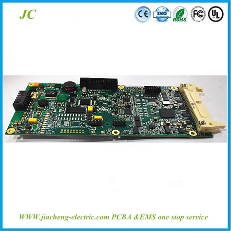
A PCBA is a PCB that has been populated with electronic components, such as resistors, capacitors, integrated circuits (ICs), and connectors. The components are soldered onto the PCB using various techniques, such as through-hole or surface-mount technology (SMT). The PCBA is the final product that is integrated into the electronic device.
Applications of PCB and PCBA
PCBs and PCBAs are used in a wide range of devices across various industries. Some of the most common applications include:
Consumer Electronics
- Smartphones and tablets
- Laptops and desktop computers
- Televisions and displays
- Gaming consoles
- Wearables (e.g., smartwatches, fitness trackers)
- Home appliances (e.g., refrigerators, washing machines, microwave ovens)
Automotive Electronics
- Engine control units (ECUs)
- Infotainment systems
- Advanced driver assistance systems (ADAS)
- Electric vehicle (EV) battery management systems
- Lighting control systems
Industrial Electronics
- Process control systems
- Programmable logic controllers (PLCs)
- Human-machine interfaces (HMIs)
- Sensors and actuators
- Power supplies and converters
Medical Electronics
- Diagnostic imaging equipment (e.g., MRI, CT, X-ray machines)
- Patient monitoring systems
- Implantable devices (e.g., pacemakers, cochlear implants)
- Surgical instruments
- Wearable health monitoring devices
Aerospace and Defense Electronics
- Avionics systems
- Radar and communication systems
- Satellite systems
- Missile guidance systems
- Unmanned aerial vehicles (UAVs)
Telecommunications
- Networking equipment (e.g., routers, switches)
- Wireless communication devices (e.g., base stations, antennas)
- Fiber optic systems
- Satellite communication systems

Benefits of Using PCBs and PCBAs
PCBs and PCBAs offer several advantages over traditional point-to-point wiring and breadboard prototyping:
-
Compact size: PCBs allow for the miniaturization of electronic devices by providing a dense, space-efficient means of interconnecting components.
-
Reliability: Properly designed and manufactured PCBs and PCBAs offer high reliability, as the connections are stable and less prone to failures compared to manual wiring.
-
Consistency: PCBs and PCBAs ensure consistent performance across multiple units, as the manufacturing process is automated and standardized.
-
Cost-effectiveness: Mass production of PCBs and PCBAs is cost-effective, as the automated manufacturing process reduces labor costs and minimizes human errors.
-
Improved signal integrity: PCBs can be designed to maintain signal integrity by minimizing electromagnetic interference (EMI) and crosstalk between traces.

PCB and PCBA Design Considerations
When designing PCBs and PCBAs for various devices, several factors must be considered to ensure optimal performance, reliability, and manufacturability:
Component Selection
Choose components that meet the electrical, thermal, and mechanical requirements of the device. Consider factors such as power rating, tolerance, package size, and availability.
Layout and Routing
Design the PCB layout to minimize signal interference, ensure proper grounding, and provide adequate cooling for heat-generating components. Follow best practices for trace width, spacing, and via placement.
Manufacturing Constraints
Consider the limitations of the PCB manufacturing process, such as minimum trace width, spacing, and hole size. Adhere to the design rules specified by the PCB manufacturer to ensure manufacturability.
Testing and Validation
Incorporate test points and debug interfaces into the PCB design to facilitate testing and validation of the assembled PCBA. Consider using boundary scan testing (JTAG) for complex designs.
Compliance and Certifications
Ensure that the PCB and PCBA design complies with relevant industry standards and regulations, such as UL, CE, FCC, and RoHS. Obtain necessary certifications for the target market and application.

PCB and PCBA Manufacturing Process
The manufacturing process for PCBs and PCBAs involves several steps:
- PCB Fabrication:
- Substrate preparation
- Copper cladding
- Photoresist application
- Exposure and development
- Etching
- Drill holes
- Solder mask application
-
Silkscreen printing
-
PCB Assembly (PCBA):
- Solder paste application
- Component placement (SMT or through-hole)
- Reflow soldering (for SMT) or wave soldering (for through-hole)
- Inspection and testing
- Conformal coating (if required)
Future Trends in PCB and PCBA Technology
As electronic devices continue to advance, PCB and PCBA technology must evolve to meet new challenges and requirements:
Miniaturization
The demand for smaller, more compact devices will drive the development of advanced packaging techniques, such as 3D packaging, chip-on-board (CoB), and system-in-package (SiP).
High-Speed and High-Frequency Applications
With the increasing adoption of 5G, IoT, and automotive radar systems, PCBs and PCBAs will need to support higher frequencies and data rates. This will require the use of advanced materials, such as low-loss dielectrics and high-conductivity copper.
Flexible and Stretchable Electronics
Flexible and stretchable PCBs will enable the development of wearable devices, medical implants, and conformable sensors. These PCBs use materials such as polyimide or thermoplastic polyurethane (TPU) as the substrate.
Sustainable and Eco-Friendly Materials
As environmental concerns grow, there will be a push for the use of eco-friendly materials in PCB and PCBA manufacturing, such as halogen-free flame retardants and lead-free solders.
Embedded Components
Embedding passive components, such as resistors and capacitors, within the PCB substrate can further reduce the size and improve the performance of electronic devices.
Frequently Asked Questions (FAQ)
-
What is the difference between a PCB and a PCBA?
A PCB is the bare board with copper traces, while a PCBA is a PCB that has been populated with electronic components and soldered. -
Can PCBs be repaired if they malfunction?
In some cases, PCBs can be repaired by replacing faulty components or repairing damaged traces. However, the feasibility of repair depends on the extent of the damage and the accessibility of the affected area. -
What is the typical lifespan of a PCB or PCBA?
The lifespan of a PCB or PCBA depends on various factors, such as the operating environment, power consumption, and component quality. Generally, a well-designed and manufactured PCB or PCBA can last for several years to decades, depending on the application. -
How can I ensure the quality of my PCB or PCBA?
To ensure the quality of your PCB or PCBA, work with reputable design and manufacturing partners who follow industry standards and best practices. Implement a robust testing and inspection process, including visual inspection, automated optical inspection (AOI), and functional testing. -
What is the typical turnaround time for PCB and PCBA manufacturing?
The turnaround time for PCB and PCBA manufacturing varies depending on the complexity of the design, the order quantity, and the manufacturing partner. Typical lead times range from a few days to several weeks, with expedited options available for time-critical projects.
Conclusion
PCBs and PCBAs are the backbone of modern electronic devices, enabling the creation of compact, reliable, and cost-effective products across various industries. As technology continues to advance, PCB and PCBA design and manufacturing must evolve to meet new challenges and requirements. By understanding the applications, benefits, and design considerations of PCBs and PCBAs, engineers and manufacturers can create innovative and high-quality electronic devices that meet the needs of an increasingly connected world.
| PCB and PCBA Applications | Benefits |
|---|---|
| Consumer Electronics | Compact size |
| Automotive Electronics | Reliability |
| Industrial Electronics | Consistency |
| Medical Electronics | Cost-effectiveness |
| Aerospace and Defense Electronics | Improved signal integrity |
| Telecommunications |
As the demand for advanced electronic devices grows, the importance of PCBs and PCBAs will only continue to increase. By staying up-to-date with the latest trends and technologies in PCB and PCBA design and manufacturing, companies can remain competitive and deliver cutting-edge products to their customers.


Leave a Reply