Introduction to PCBA Manufacturing
Printed Circuit Board Assembly (PCBA) manufacturing is a complex process that involves the assembly of electronic components onto a printed circuit board (PCB). The PCB is the backbone of every electronic device, and the quality of the PCBA determines the overall performance and reliability of the final product. In this comprehensive guide, we will walk you through the step-by-step process of PCBA manufacturing, from design to final assembly.
The PCBA Manufacturing Process
The PCBA manufacturing process consists of several stages, each of which is critical to ensuring the quality and reliability of the final product. The following table outlines the main stages of the PCBA manufacturing process:
| Stage | Description |
|---|---|
| Design | The PCB design is created using specialized software, taking into account the specific requirements of the final product. |
| Fabrication | The PCB is fabricated using a variety of techniques, including etching, drilling, and plating. |
| Component Placement | The electronic components are placed onto the PCB using automated pick-and-place machines. |
| Soldering | The components are soldered onto the PCB using either through-hole or surface-mount technology. |
| Inspection | The assembled PCBA is inspected for quality and functionality using automated optical inspection (AOI) and other techniques. |
| Testing | The PCBA is tested for performance and reliability using a variety of methods, including in-circuit testing (ICT) and functional testing. |
| Finishing | The PCBA is finished with any necessary coatings or treatments, such as conformal coating or potting. |
Step 1: PCB Design
The first step in the PCBA manufacturing process is the design of the PCB. This is typically done using specialized software, such as Altium Designer or Eagle. The PCB design takes into account the specific requirements of the final product, including the number and type of components, the size and shape of the board, and any necessary connectors or other features.
Important Considerations in PCB Design
When designing a PCB, there are several important considerations to keep in mind, including:
- Component placement: The placement of components on the board should be optimized for ease of assembly and reliability.
- Signal integrity: The PCB design should minimize signal interference and ensure that all signals are properly terminated.
- Thermal management: The PCB design should take into account the thermal requirements of the components and provide adequate cooling.
- Manufacturing constraints: The PCB design should be optimized for manufacturability, taking into account the capabilities and limitations of the manufacturing process.
Step 2: PCB Fabrication
Once the PCB design is complete, the next step is to fabricate the board. This involves a variety of techniques, including:
- Etching: The copper traces on the board are etched using a chemical process.
- Drilling: Holes are drilled in the board for through-hole components and vias.
- Plating: The holes are plated with copper to ensure good electrical conductivity.
- Solder mask application: A solder mask is applied to the board to protect the copper traces and prevent short circuits.
- Silkscreen printing: Text and other markings are printed on the board using a silkscreen process.
Types of PCB Fabrication
There are several different types of PCB fabrication, each with its own advantages and disadvantages. The most common types are:
- Single-sided: A single-sided PCB has copper traces on only one side of the board.
- Double-sided: A double-sided PCB has copper traces on both sides of the board.
- Multi-layer: A multi-layer PCB has multiple layers of copper traces separated by insulating material.
- Flexible: A flexible PCB is made from a flexible material, such as polyimide, and can be bent or folded as needed.
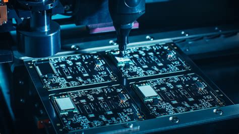
Step 3: Component Placement
Once the PCB has been fabricated, the next step is to place the electronic components onto the board. This is typically done using automated pick-and-place machines, which can place components onto the board with high speed and accuracy.
Types of Components
There are many different types of electronic components that can be used in a PCBA, including:
- Resistors: Used to limit current flow and provide resistance in a circuit.
- Capacitors: Used to store electrical charge and filter out noise in a circuit.
- Inductors: Used to store energy in a magnetic field and filter out high-frequency signals.
- Diodes: Used to allow current to flow in only one direction and protect against voltage spikes.
- Transistors: Used to amplify or switch electronic signals.
- Integrated circuits (ICs): Complex electronic circuits that are packaged into a single chip.
Placement Techniques
There are two main techniques used for placing components onto a PCB:
- Through-hole technology (THT): Components are inserted into holes drilled in the PCB and soldered in place.
- Surface-mount technology (SMT): Components are placed directly onto the surface of the PCB and soldered in place.
SMT is generally preferred over THT for most applications, as it allows for higher component density and faster assembly times. However, THT may still be used for certain types of components or in applications where high reliability is critical.
Step 4: Soldering
Once the components have been placed onto the PCB, the next step is to solder them in place. Soldering is the process of joining two or more metal surfaces by melting a filler metal (solder) between them.
Types of Soldering
There are two main types of soldering used in PCBA manufacturing:
- Wave soldering: The PCB is passed over a wave of molten solder, which flows up through the holes in the board and solders the components in place.
- Reflow soldering: The PCB is heated in an oven, causing the solder paste to melt and flow around the components, soldering them in place.
Reflow soldering is generally preferred over wave soldering for SMT components, as it allows for more precise control over the soldering process and can accommodate smaller components and tighter spacing.
Soldering Defects
Soldering defects can occur during the soldering process, which can lead to poor electrical connections and reduced reliability. Some common soldering defects include:
- Bridging: Solder flows between adjacent pads or traces, creating a short circuit.
- Cold joints: Solder does not flow properly, resulting in a weak or incomplete connection.
- Tombstoning: One end of a component lifts off the PCB during soldering, resulting in an open circuit.
- Insufficient or excessive solder: Too little or too much solder is used, resulting in a weak or bulky connection.
Proper process control and inspection are critical to minimizing soldering defects and ensuring the quality and reliability of the final product.
Step 5: Inspection
After the components have been soldered onto the PCB, the next step is to inspect the assembled PCBA for quality and functionality. This is typically done using a combination of automated inspection equipment and manual inspection by trained operators.
Automated Optical Inspection (AOI)
AOI is a type of automated inspection that uses cameras and image processing software to inspect the PCBA for defects. AOI systems can detect a wide range of defects, including:
- Missing or misaligned components
- Solder defects, such as bridges or insufficient solder
- Incorrect component values or orientations
- Damaged or lifted pads or traces
AOI is a fast and accurate method of inspection that can catch defects that may be missed by manual inspection. However, it is not foolproof and may not catch all types of defects.
Manual Inspection
Manual inspection is still an important part of the PCBA inspection process, particularly for complex or high-reliability applications. Trained operators use magnifying lenses and other tools to visually inspect the PCBA for defects that may be missed by AOI.
Manual inspection is slower and more labor-intensive than AOI, but it can catch certain types of defects that may be missed by automated inspection, such as subtle solder defects or component damage.
Step 6: Testing
Once the PCBA has been inspected for defects, the next step is to test it for performance and functionality. Testing is critical to ensuring that the PCBA meets the required specifications and will perform reliably in the final product.
In-Circuit Testing (ICT)
ICT is a type of testing that uses a bed-of-nails fixture to make electrical contact with specific points on the PCBA. The fixture is connected to a computer-controlled test system that can measure various parameters, such as resistance, capacitance, and voltage.
ICT can detect a wide range of defects, including:
- Short circuits or open circuits
- Incorrect component values or orientations
- Damaged or missing components
- Solder defects
ICT is a fast and accurate method of testing that can catch defects that may be missed by other testing methods. However, it requires specialized equipment and fixtures, which can be expensive to develop and maintain.
Functional Testing
Functional testing involves testing the PCBA under real-world operating conditions to ensure that it performs as intended. This may involve connecting the PCBA to other components or systems and running various test scenarios to verify functionality.
Functional testing can catch defects that may not be detected by ICT or other testing methods, such as software bugs or compatibility issues. However, it is typically more time-consuming and may require specialized test equipment or fixtures.
Step 7: Finishing
After the PCBA has been tested and verified for functionality, the final step is to apply any necessary finishing treatments to protect the board and components from environmental factors such as moisture, dust, or corrosion.
Conformal Coating
Conformal coating is a type of protective coating that is applied to the surface of the PCBA to protect it from moisture, dust, and other contaminants. There are several types of conformal coatings, including:
- Acrylic: A clear, hard coating that provides good moisture and abrasion resistance.
- Silicone: A flexible, rubbery coating that provides good thermal and chemical resistance.
- Urethane: A tough, durable coating that provides excellent moisture and chemical resistance.
Conformal coating is typically applied using a spray or dip process and can be cured using heat or UV light.
Potting
Potting involves encapsulating the PCBA in a solid compound, such as epoxy or silicone, to provide additional protection from environmental factors and physical damage. Potting is typically used in applications where the PCBA may be exposed to harsh conditions, such as high temperatures or vibration.
Potting can provide excellent protection for the PCBA, but it can also make repairs or modifications more difficult and may require specialized equipment for application.

Frequently Asked Questions (FAQ)
What is the difference between PCB and PCBA?
A PCB (printed circuit board) is the bare board without any components attached, while a PCBA (printed circuit board assembly) is the complete assembly with all the components soldered onto the board.
What are the advantages of surface-mount technology (SMT) over through-hole technology (THT)?
SMT allows for higher component density, faster assembly times, and better performance at high frequencies compared to THT. However, THT may still be used for certain types of components or in applications where high reliability is critical.
What types of defects can occur during the soldering process?
Common soldering defects include bridging (solder flowing between adjacent pads or traces), cold joints (weak or incomplete connections), tombstoning (one end of a component lifting off the PCB), and insufficient or excessive solder.
What is the purpose of automated optical inspection (AOI)?
AOI uses cameras and image processing software to automatically inspect the PCBA for defects such as missing or misaligned components, solder defects, and incorrect component values or orientations.
What types of finishing treatments can be applied to a PCBA?
Common finishing treatments for PCBAs include conformal coating (a protective coating applied to the surface of the board) and potting (encapsulating the board in a solid compound for additional protection).

Conclusion
PCBA manufacturing is a complex process that involves multiple stages, from design and fabrication to assembly, inspection, testing, and finishing. Each stage plays a critical role in ensuring the quality, reliability, and functionality of the final product.
By understanding the steps involved in PCBA manufacturing and the various techniques and technologies used at each stage, designers and manufacturers can optimize their processes to minimize defects, improve efficiency, and deliver high-quality products to their customers.
As electronic devices continue to become more complex and sophisticated, the importance of PCBA manufacturing will only continue to grow. By staying up-to-date with the latest advancements in PCBA technology and best practices, manufacturers can stay competitive in an increasingly challenging market.


Leave a Reply