Introduction to Circuit Boards
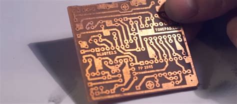
A circuit board, also known as a printed circuit board (PCB), is the backbone of modern electronic devices. It is a flat board made of insulating material, such as fiberglass or plastic, with conductive pathways etched or printed onto its surface. These pathways, called traces, connect various electronic components, such as resistors, capacitors, and integrated circuits (ICs), to form a complete electronic circuit.
Circuit boards have revolutionized the electronics industry by providing a compact, reliable, and cost-effective way to assemble electronic devices. They are used in a wide range of applications, from simple toys and household appliances to complex medical equipment, aerospace systems, and supercomputers.
Types of Circuit Boards
There are several types of circuit boards, each with its own unique characteristics and applications. The most common types include:
-
Single-sided PCBs: These boards have conductive traces on only one side of the insulating substrate. They are the simplest and most cost-effective type of PCB, suitable for low-complexity circuits.
-
Double-sided PCBs: These boards have conductive traces on both sides of the insulating substrate, allowing for more complex circuits and higher component density. The two sides are connected using vias, which are small holes drilled through the board and plated with conductive material.
-
Multi-layer PCBs: These boards consist of multiple layers of insulating material and conductive traces, sandwiched together to form a single board. They offer the highest level of circuit complexity and density, making them ideal for advanced electronic applications.
-
Flexible PCBs: These boards are made of flexible insulating material, such as polyimide, allowing them to bend and conform to various shapes. They are commonly used in applications where space is limited or where the board needs to fit into a specific form factor.
-
Rigid-Flex PCBs: These boards combine the features of rigid and flexible PCBs, consisting of rigid sections connected by flexible sections. They offer the benefits of both types of boards, providing a high level of circuit complexity and mechanical flexibility.
PCB Design and Fabrication Process
The process of creating a circuit board involves several steps, from the initial design to the final fabrication and assembly. The following sections provide an overview of each step in the process.
PCB Design
The first step in creating a circuit board is the design phase. This involves using specialized software, such as Altium Designer, Eagle, or KiCad, to create a schematic diagram and a layout of the board.
The schematic diagram represents the electrical connections between the various components, while the layout shows the physical placement of the components and the routing of the conductive traces.
During the design phase, engineers must consider several factors, such as:
- Component selection and placement
- Signal integrity and electromagnetic compatibility (EMC)
- Power distribution and thermal management
- Manufacturing constraints and design rules
PCB Fabrication
Once the design is complete, the next step is to fabricate the circuit board. This involves several processes, including:
-
Substrate preparation: The insulating substrate, typically made of fiberglass or plastic, is cut to the desired size and shape.
-
Copper cladding: A thin layer of copper is laminated onto the substrate using heat and pressure.
-
Photoresist application: A light-sensitive material, called photoresist, is applied to the copper surface.
-
Exposure and development: The photoresist is exposed to UV light through a photomask, which contains the circuit pattern. The exposed areas of the photoresist are then removed using a developer solution, leaving the desired circuit pattern on the copper surface.
-
Etching: The exposed copper is removed using an etchant solution, leaving only the desired conductive traces.
-
Drilling: Holes are drilled through the board to accommodate through-hole components and vias.
-
Plating: The holes are plated with a conductive material, such as copper, to ensure electrical continuity between layers.
-
Solder mask application: A protective coating, called solder mask, is applied to the board, covering the areas that should not be exposed to solder during the assembly process.
-
Silkscreen printing: Text, symbols, and logos are printed onto the board using a silkscreen process, providing useful information for assembly and troubleshooting.
PCB Assembly
The final step in creating a functional circuit board is the assembly process, which involves soldering the electronic components onto the board. This can be done manually or using automated equipment, such as pick-and-place machines and reflow ovens.
The most common methods of PCB assembly include:
-
Through-hole assembly: Components with long leads are inserted through holes in the board and soldered onto the opposite side.
-
Surface-mount assembly: Components with small, flat leads are placed directly onto pads on the surface of the board and soldered in place using a reflow oven.
After the components are soldered, the board undergoes a series of tests to ensure proper functionality and reliability. These tests may include visual inspection, automated optical inspection (AOI), X-ray inspection, and electrical testing.

PCB Materials and Properties
The choice of materials used in the construction of a circuit board can have a significant impact on its performance, reliability, and cost. The following sections provide an overview of the most common PCB materials and their properties.
Substrate Materials
The substrate is the insulating material that forms the base of the circuit board. The most common substrate materials include:
-
FR-4: A composite material made of fiberglass and epoxy resin, FR-4 is the most widely used substrate material for PCBs. It offers good mechanical strength, thermal stability, and electrical insulation properties.
-
Polyimide: A high-performance plastic, polyimide is used in flexible PCBs and applications that require high temperature resistance and dimensional stability.
-
Teflon: A fluoropolymer with excellent dielectric properties, Teflon is used in high-frequency and microwave applications.
-
Ceramic: Alumina and other ceramic materials are used in high-power and high-temperature applications, offering excellent thermal conductivity and electrical insulation properties.
Copper Foil
Copper foil is the conductive material used to create the traces and pads on the circuit board. The thickness of the copper foil is typically expressed in ounces per square foot (oz/ft²), with common thicknesses ranging from 0.5 oz/ft² to 2 oz/ft².
Thicker copper foil offers lower resistance and higher current-carrying capacity, but it can also increase the cost and complexity of the manufacturing process.
Solder Mask
Solder mask is a protective coating applied to the surface of the circuit board, covering the areas that should not be exposed to solder during the assembly process. It helps prevent short circuits and improves the overall reliability of the board.
Solder mask is typically made of a polymer material and is available in various colors, with green being the most common. Other colors, such as red, blue, and black, are used for specialized applications or for aesthetic purposes.
Silkscreen
Silkscreen is a printed layer on the surface of the circuit board that contains text, symbols, and logos. It provides useful information for assembly, testing, and troubleshooting, such as component designators, polarity indicators, and test points.
Silkscreen is typically printed using white ink, but other colors, such as black or yellow, may be used for improved visibility or aesthetic reasons.

PCB Design Considerations
When designing a circuit board, there are several key factors to consider to ensure optimal performance, reliability, and manufacturability. The following sections provide an overview of some of the most important design considerations.
Component Placement
The placement of components on the circuit board can have a significant impact on its performance and manufacturability. Some key considerations include:
-
Functionality: Components should be placed in a logical and intuitive manner, grouping related components together and minimizing the distance between them to reduce signal delays and improve noise immunity.
-
Mechanical constraints: The placement of components must take into account the mechanical constraints of the board, such as the location of mounting holes, connectors, and other mechanical features.
-
Thermal management: High-power components, such as voltage regulators and power transistors, should be placed in a way that allows for adequate heat dissipation, using thermal vias, heatsinks, or other cooling methods as necessary.
-
Manufacturing: The placement of components must be compatible with the manufacturing process, ensuring adequate clearance for pick-and-place machines and avoiding areas that may be difficult to access during soldering or inspection.
Routing and Signal Integrity
The routing of traces on the circuit board is critical for ensuring signal integrity and minimizing noise and interference. Some key considerations include:
-
Trace width and spacing: The width and spacing of traces must be carefully designed to ensure adequate current-carrying capacity and to minimize crosstalk and electromagnetic interference (EMI).
-
Impedance control: In high-speed and high-frequency applications, the impedance of traces must be carefully controlled to minimize reflections and ensure proper signal termination.
-
Grounding and shielding: Proper grounding and shielding techniques must be used to minimize noise and interference, using ground planes, guard traces, and shielded enclosures as necessary.
-
Length matching: In applications where timing is critical, such as in digital systems, the length of traces must be carefully matched to ensure proper signal synchronization and minimize skew.
Power Distribution
The distribution of power on the circuit board is another critical design consideration, particularly in high-power and high-speed applications. Some key considerations include:
-
Power plane: The use of a dedicated power plane, typically on an inner layer of the board, can help provide a low-impedance path for power distribution and minimize voltage drops and noise.
-
Decoupling capacitors: The placement of decoupling capacitors close to power-consuming components can help reduce noise and ensure a stable power supply.
-
Voltage regulation: The use of voltage regulators and other power management techniques can help ensure a stable and clean power supply, particularly in applications with sensitive analog or digital circuits.
Electromagnetic Compatibility (EMC)
Electromagnetic compatibility (EMC) refers to the ability of a circuit board to operate reliably in the presence of electromagnetic interference (EMI) and to minimize its own emissions. Some key considerations include:
-
Grounding and shielding: Proper grounding and shielding techniques, such as the use of ground planes and shielded enclosures, can help minimize EMI and improve EMC.
-
Filtering: The use of filters, such as ferrite beads and capacitors, can help suppress high-frequency noise and improve EMC.
-
Component selection: The choice of components, particularly those with low EMI emissions or high immunity to interference, can help improve the overall EMC of the board.
-
Layout and routing: The layout and routing of the board, particularly the placement of high-frequency components and the routing of sensitive signals, can have a significant impact on EMC.
Design for Manufacturing (DFM)
Design for manufacturing (DFM) refers to the process of designing a circuit board in a way that is compatible with the manufacturing process and ensures high yields and reliability. Some key considerations include:
-
Design rules: Adhering to the design rules provided by the PCB manufacturer, such as minimum trace width and spacing, hole size, and clearance, can help ensure manufacturability and minimize defects.
-
Panelization: The layout of the board should be designed to allow for efficient panelization, minimizing waste and ensuring compatibility with the manufacturing equipment.
-
Testability: The board should be designed with testability in mind, incorporating test points, fiducials, and other features that facilitate automated testing and inspection.
-
Component selection: The choice of components should take into account their availability, cost, and compatibility with the manufacturing process, avoiding obsolete or hard-to-source components whenever possible.

PCB Testing and Inspection
After the circuit board has been manufactured and assembled, it must undergo a series of tests and inspections to ensure proper functionality and reliability. The following sections provide an overview of some of the most common testing and inspection methods.
Visual Inspection
Visual inspection is the most basic form of PCB testing, involving a manual or automated visual examination of the board for defects such as missing or misaligned components, solder bridges, and damaged traces.
Manual visual inspection is typically performed using a magnifying lens or microscope, while automated visual inspection uses machine vision systems and image processing algorithms to detect defects.
Automated Optical Inspection (AOI)
Automated optical inspection (AOI) is a more advanced form of visual inspection that uses high-resolution cameras and image processing software to detect defects on the surface of the board.
AOI systems can detect a wide range of defects, including missing or misaligned components, solder bridges, and damaged traces, and can provide detailed reports and statistics on the quality of the board.
X-Ray Inspection
X-ray inspection is used to detect defects that are not visible on the surface of the board, such as voids in solder joints, missing or misaligned components on the bottom side of the board, and internal delamination or cracking.
X-ray inspection systems use high-energy X-rays to penetrate the board and create a detailed image of its internal structure, allowing for the detection of defects that would otherwise be hidden from view.
In-Circuit Testing (ICT)
In-circuit testing (ICT) is a form of electrical testing that involves directly probing the nodes and components on the board to verify their functionality and connectivity.
ICT systems use a bed-of-nails fixture that makes contact with the test points on the board, allowing for the measurement of resistance, capacitance, and other electrical parameters.
ICT can detect a wide range of defects, including open and short circuits, incorrect component values, and missing or damaged components.
Functional Testing
Functional testing involves powering up the board and verifying its operation under normal conditions, typically using automated test equipment (ATE) or a custom test fixture.
Functional testing can detect defects that are not visible or detectable using other testing methods, such as timing or signal integrity issues, software bugs, or performance problems.
Functional testing may involve a range of tests, such as boundary scan testing, signal integrity testing, and burn-in testing, depending on the specific requirements of the application.
PCB Troubleshooting and Repair
Despite the best efforts of designers and manufacturers, circuit boards can still fail or malfunction in the field. When this happens, it is important to have a systematic approach to troubleshooting and repair to minimize downtime and ensure reliable operation.
The following sections provide an overview of some of the most common troubleshooting and repair techniques.
Visual Inspection
As with testing, visual inspection is the first step in troubleshooting a malfunctioning circuit board. This involves carefully examining the board for signs of damage, such as burnt or discolored components, cracked or lifted traces, or damaged connectors.
Visual inspection can often provide clues as to the nature and location of the problem, allowing for more targeted troubleshooting and repair efforts.
Continuity Testing
Continuity testing involves using a multimeter or other test equipment to verify the electrical continuity of traces, vias, and connectors on the board.
This can help identify open circuits, short circuits, or high-resistance connections that may be causing the malfunction.
Continuity testing is typically performed using a low-voltage, low-current signal to avoid damaging the board or its components.
Component Testing
Component testing involves verifying the functionality and performance of individual components on the board, such as resistors, capacitors, and integrated circuits.
This can be done using a variety of test equipment, such as multimeters, oscilloscopes, and logic analyzers, depending on the specific component and the nature of the problem.
Component testing can help identify faulty or out-of-spec components that may be causing the malfunction, allowing for targeted replacement or repair.
Signal Tracing
Signal tracing involves using an oscilloscope or other test equipment to monitor the signals on the board and verify their integrity and timing.
This can help identify signal integrity issues, such as reflections, crosstalk, or noise, that may be causing the malfunction.
Signal tracing can also help identify the source of the problem, such as a faulty component or a design flaw, allowing for more targeted troubleshooting and repair efforts.
Rework and Repair
Once the source of the problem has been identified, the next step is to perform the necessary rework or repair to fix the issue.
This may involve replacing faulty components, repairing damaged traces or vias, or modifying the board layout or design to address signal integrity or other issues.
Rework and repair can be a delicate and time-consuming process, requiring specialized tools and techniques to avoid damaging the board or its components.
In some cases, it may be more cost-effective to replace the entire board rather than attempting to repair it, particularly if the board is old or obsolete, or if the repair requires extensive rework or modification.
Common PCB Defects and Failures
Despite the best efforts of designers and manufacturers, circuit boards can still suffer from a variety of defects and failures that can impact their performance and reliability.
The following table provides an overview of some of the most common PCB defects and failures, along with their causes and potential remedies:
| Defect/Failure | Description | Causes | Potential Remedies |
|---|---|---|---|
| Solder bridges | Unintended connections between adjacent pads or traces | Excess solder, poor solder mask coverage, improper soldering technique | Solder wick, solder sucker, manual rework |
| Cold solder joints | Dull, grainy, or incomplete solder joints that may be prone to cracking or failure | Insufficient heat, improper soldering technique, contaminated or oxidized surfaces | Reflow soldering, manual |


Leave a Reply