Introduction
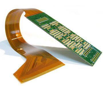
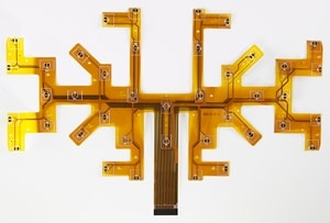
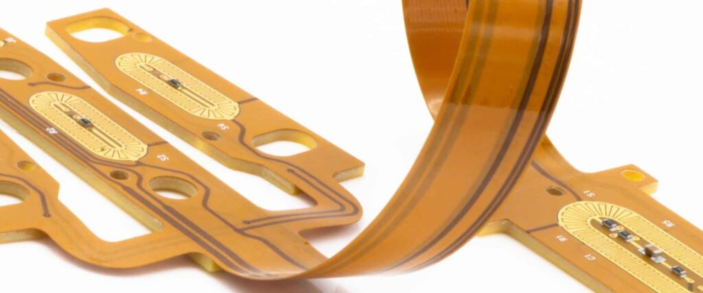
Printed circuit boards (PCBs) are essential components in modern electronics. Increasingly, products require complex and compact PCB designs that can fit into tight spaces. This has led to the rise in popularity of flexible PCBs, rigid-flex PCBs, and flex circuits.
These types of PCBs can bend and flex to accommodate unique product enclosures. They provide more freedom for routing traces and placing components. Rigid-flex PCBs combine standard rigid PCB sections with flexible sections that connect them. The flexible sections allow the rigid sections to bend or fold as needed.
Altium is a leading PCB design software that provides extensive tools for designing flexible and rigid-flex PCBs. One of these is the bending line, which defines the flexible areas of a rigid-flex design. This article will examine how to utilize the bending line tool in Altium to create advanced flexible and rigid-flex designs.
What is a Bending Line in Altium?
In Altium, a bending line represents where a rigid-flex PCB can bend or fold. It divides the rigid sections of the PCB from the flexible sections. Bending lines display on the 2D and 3D views of the PCB layout. They also interact with the layer stack to properly configure the stackup in rigid and flex areas.
The software essentially treats the rigid and flex regions divided by the bending line as separate PCBs with different layer stacks. This allows you to define different layer stacks in the rigid and flex areas, an essential requirement for rigid-flex designs.
Key Properties of the Bending Line
Below are some of the key properties of a bending line in Altium:
- Bending Length – The length along the bending line that will actually flex or bend. This can be shorter than the total line length.
- Bend Radius – The radius the PCB will bend through at the bending line. The minimum depends on the layers and materials.
- Layer Stack – The separate layer stacks defined in the rigid and flex regions. Allows different layer configurations.
- Teardrop Pads – Optional teardrop-shaped pads placed at bending line junctions for flexibility.
- Routing Topology – The PCB bending shape like a fold, coil or arc. Determines the line shape.
Creating a Bending Line
Step 1. – With your rigid-flex PCB design open in Altium, switch to the 2D Layout mode. Go to Design > Layer Stack Manager and define layer stacks for the rigid and flex sections.
Step 2. – Go to Design > Define Bending Line or click the bending line icon. Then choose either an Arc or Polygon bending line shape.
Step 3. – Draw the bending line on the 2D layout. Use vertices to create the required shape according to the PCB outline.
Step 4. – With the bending line still selected, configure the key properties in the Properties panel, including Bending Length, Bend Radius, Layer Stack and Routing Topology.
Step 5. – Save the bending line. The software will update the layer stack on either side and add teardrop pads if selected. Your rigid-flex design is now configured!
Configuring Layer Stacks
A key part of any rigid-flex design is configuring the layer stack densities in the rigid and flex regions. Here are some guidelines:
- Rigid sections can have a higher layer count with prepreg/core layers. Flex sections need thinner stackups.
- Minimize layer count in the flex area as much as possible. 2-6 layers is common.
- Ensure flex bend areas have bare minimum layer count, such as 1-2 layers.
- Match the layer types (signal/plane) on either side of the bending line.
Use the Layer Stack Manager in Altium to easily configure the layer densities in the rigid and flex regions. The bending line will automatically divide and assign the layer stacks.
Routing Considerations
Routing traces across a bending line requires special considerations:
- Minimize trace count in the bending area. Keep critical signals only.
- Use teardrop pads at trace junctions for stress relief. Altium can auto-add teardrops.
- Avoid having traces run perpendicular to the bending line. Use 45 degree angles.
- Where possible, run traces in the outer layers. This reduces stress from bending.
- Account for thickness changes when routing across the bending line.
Analyzing Bending Line Clearances
In a complex rigid-flex PCB, it is important to analyze the bending line clearances. Set up rigid-flex rules in the PCB Rules and Constraints Editor. Some key checks include:
- Check minimum electrical clearance between layers at the bend areas.
- Verify component clearance from bending lines for range of motion needed.
- Confirm bend radius meets requirements for flex layers used.
- Analyze forces and stresses on traces crossing bending lines.
Running the design rule check will validate all rigid-flex requirements. The 3D viewer can also assist in visually checking clearances as the PCB is flexed.
Producing Rigid-Flex PCBs
Once finished, the rigid-flex design can move to production. The Gerber outputs will include the bending lines so manufacturers know where the PCB can flex. Here are some manufacturing notes:
- Work with manufacturers familiar with rigid-flex PCB processes. Requirements are more stringent.
- Specify materials carefully. Flexible layers require different materials from rigid layers.
- Expect higher costs than standard PCBs due to specialized materials and processes.
- There may be limitations based on flex layer thickness and bend radii.
- Expect longer lead times for assembly and testing.
With careful design, review and manufacturing, rigid-flex PCBs designed in Altium can become realities and enable amazing electronic products. The bending line tool facilitates the specialized requirements of flexible circuits.
Frequently Asked Questions
What are the key benefits of a rigid-flex PCB design?
Some benefits include:
- Ability to fit PCBs into tight spaces by bending/folding
- Higher component density with flexible layer routing
- Reduced system wiring vs connecting separate PCBs
- Eliminates interboard connectors
- Improved reliability with fewer interconnections
- Reduces assembly cost
What special design rules apply for rigid-flex PCBs?
Key rigid-flex design rules:
- Different layer stacks in rigid vs flex areas
- Minimum trace widths based on flex material and layers
- Limits on number of layers in bend areas
- Minimum electrical clearance for multilayer bends
- Teardrop pads at trace junctions across bends
- Minimal trace routing perpendicular to bending line
How are components placed on rigid-flex PCBs?
- Components go only on rigid sections, not on flexible areas.
- Ensure components have clearance from bending lines for required range of flex motion.
- Place components on outer rigid layers where possible.
- Use smaller, micro-packaged components. Standard components may be too big.
What are some examples of products using rigid-flex PCBs?
- Mobile phones
- Laptop and tablet computers
- Printers
- Hard disk drives
- Medical devices
- Aerospace and military products
- Automotive cameras
What are the typical failure modes of rigid-flex PCBs?
- Excessive bending leading to cracked traces
- Broken solder joints due to repeated flexing
- Fractured plating at flex/bend junctions
- Flexible substrate delamination
- Cracked passivation layer allowing corrosion
- Loss of electrical clearance at bend sites
Summary
The bending line in Altium provides powerful functionality for designing flexible and rigid-flex PCBs. It allows defining the rigid and flex sections including their unique layer stacks. With the right design rules and manufacturing approach, rigid-flex PCBs enable highly advanced and compact products. Utilizing Altium’s tools facilitates creating designs that can withstand the rigors of flexing and bending during product use.


Leave a Reply