Planning and Design Techniques
Create a Detailed Schematic
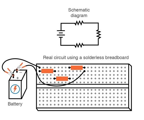
Before you start building your circuit board, it’s crucial to create a detailed schematic. This schematic should include all the components, their values, and how they connect. Use software like KiCad, Eagle, or Altium Designer to create your schematic.
Choose the Right PCB Layout Software
Selecting the right PCB layout software is key to designing an efficient and effective circuit board. Popular options include:
| Software | Pros | Cons |
|---|---|---|
| KiCad | Free, open-source, cross-platform | Steeper learning curve |
| Eagle | User-friendly, large component library | Limited free version |
| Altium Designer | Powerful features, industry standard | Expensive |
Consider your needs, budget, and experience level when choosing PCB layout software.
Consider PCB Size and Shape
The size and shape of your PCB will depend on its purpose and the space constraints of your project. Keep these factors in mind:
- Component placement
- Mounting requirements
- Enclosure size
- Connectors and interfaces
Optimize your PCB layout to minimize size while ensuring proper functionality and ease of assembly.
PCB Fabrication Techniques
Choose the Right Substrate Material
The substrate material you choose for your PCB will impact its performance, durability, and cost. Common substrate materials include:
- FR-4: Most popular, good balance of properties and cost
- Aluminum: Excellent thermal conductivity, used for heat dissipation
- Polyimide: High temperature resistance, flexible
Select the substrate material that best suits your project’s requirements.
Determine the Number of Layers
The number of layers in your PCB will affect its complexity, cost, and signal integrity. Use the following guidelines:
| Layers | Application |
|---|---|
| 1-2 | Simple, low-cost projects |
| 4 | Most common for moderate complexity |
| 6+ | High-speed, high-density designs |
More layers allow for better signal routing and power distribution but increase fabrication costs.
Specify the Copper Thickness
Copper thickness, measured in ounces per square foot (oz/ft²), determines the current-carrying capacity and impedance of your PCB traces. Typical values are:
- 0.5 oz/ft²: Used for low-power, high-density designs
- 1 oz/ft²: Most common, suitable for general-purpose applications
- 2 oz/ft²: Used for high-current or high-power designs
Thicker copper allows for higher current capacity but can make PCB fabrication more challenging.

Assembly Techniques
Use Proper Soldering Techniques
Soldering is a critical skill for assembling circuit boards. Follow these tips for success:
- Use the right soldering iron and tip for your components
- Apply the appropriate amount of heat and solder
- Ensure proper joint formation and avoid bridging or cold joints
- Clean your soldering iron tip regularly
Practice proper soldering techniques to ensure reliable connections and avoid damaging components.
Consider Surface Mount Technology (SMT)
Surface mount technology (SMT) offers several advantages over through-hole mounting:
- Smaller component sizes
- Increased component density
- Faster assembly using automated processes
However, SMT requires specialized equipment and can be more challenging for manual assembly.
Use Proper Component Placement and Orientation
When placing components on your PCB, consider the following:
- Group related components together for easier routing and signal integrity
- Orient components to minimize trace lengths and crossovers
- Ensure proper clearance between components for soldering and heat dissipation
- Follow manufacturer recommendations for component placement and orientation
Proper component placement and orientation will simplify PCB assembly and improve overall performance.

Testing and Debugging Techniques
Perform Visual Inspections
Before powering on your circuit board, perform a thorough visual inspection:
- Check for proper component placement and orientation
- Look for solder bridges, cold joints, or missing solder
- Verify correct polarity of polarized components
- Ensure there are no foreign objects or debris on the board
Visual inspections can catch many common issues and prevent damage to your PCB.
Use Multimeters and Oscilloscopes
Multimeters and oscilloscopes are essential tools for testing and debugging your circuit board:
- Multimeters measure voltage, current, and resistance
- Oscilloscopes display waveforms and signal timing
Use these tools to:
- Verify power supply voltages
- Check for shorts or open circuits
- Measure signal levels and timing
- Identify noise or interference issues
Proficiency with multimeters and oscilloscopes will greatly enhance your ability to troubleshoot and debug PCBs.
Employ Modular Testing
When debugging complex circuit boards, employ a modular testing approach:
- Divide the circuit into functional blocks
- Test each block individually, verifying inputs and outputs
- Gradually integrate blocks and test their interactions
- Isolate and focus on problem areas
Modular testing helps isolate issues and simplifies the debugging process.

Frequently Asked Questions (FAQ)
What is the best software for designing PCBs?
The best PCB design software depends on your needs, budget, and experience level. Popular options include KiCad (free, open-source), Eagle (user-friendly, large component library), and Altium Designer (powerful, industry standard).
How do I choose the right substrate material for my PCB?
Consider your project’s requirements for performance, durability, and cost. FR-4 is the most common substrate material, offering a good balance of properties. Aluminum provides excellent thermal conductivity, while polyimide is used for high-temperature or flexible applications.
What are the advantages of surface mount technology (SMT)?
SMT offers several advantages over through-hole mounting, including smaller component sizes, increased component density, and faster assembly using automated processes. However, SMT requires specialized equipment and can be more challenging for manual assembly.
How can I improve my soldering skills?
To improve your soldering skills, practice regularly with the right tools and techniques. Use the appropriate soldering iron and tip for your components, apply the right amount of heat and solder, ensure proper joint formation, and clean your soldering iron tip regularly. Practice on scrap boards or soldering practice kits to refine your technique.
What are the essential tools for testing and debugging circuit boards?
Essential tools for testing and debugging circuit boards include multimeters and oscilloscopes. Multimeters measure voltage, current, and resistance, while oscilloscopes display waveforms and signal timing. Use these tools to verify power supply voltages, check for shorts or open circuits, measure signal levels and timing, and identify noise or interference issues.
By mastering these 11 essential Circuit Building Techniques, you’ll be well-equipped to design, fabricate, assemble, and debug high-quality PCBs for your projects. Remember to continually practice and refine your skills to stay current with the latest technologies and best practices in the ever-evolving world of electronics.


Leave a Reply