Introduction
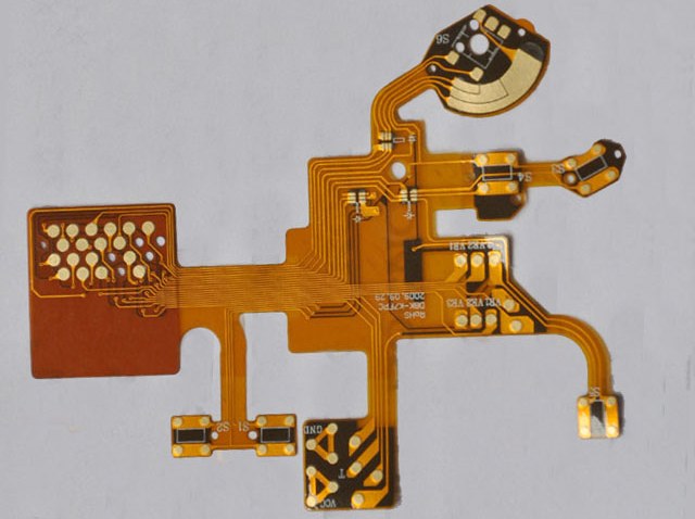
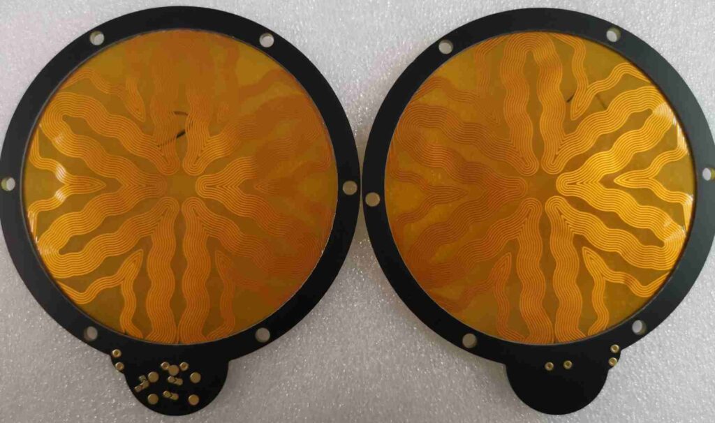
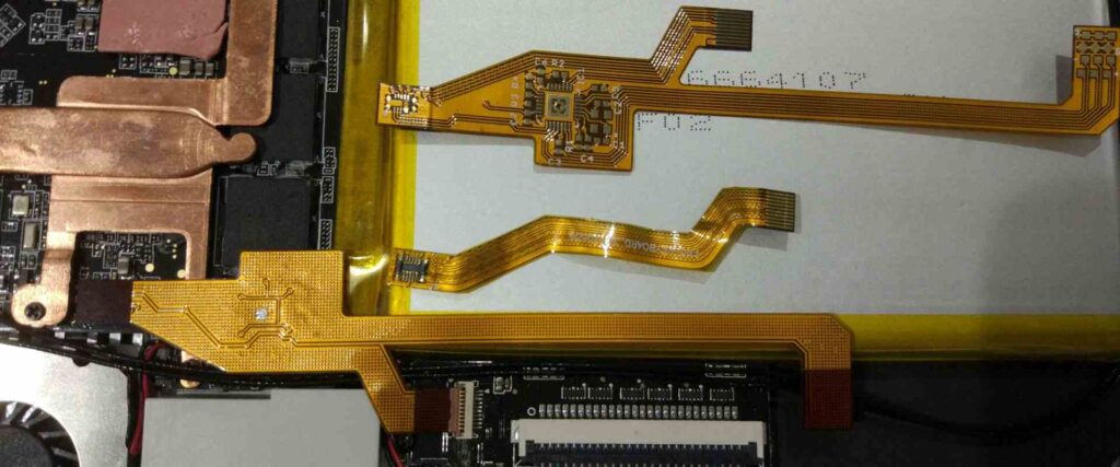
Flex PCBs, also known as flexible printed circuit boards, are circuit boards made of flexible dielectric materials such as polyimide. Flex PCBs can be bent and twisted without causing damage to the copper traces, allowing them to conform to three-dimensional product enclosures.
6 layer flex PCBs contain 6 conductive copper layers separated by 5 dielectric layers. The multiple conductive layers allow complex circuitry and dense component layouts to be packed into a very thin profile, making 6 layer flex PCBs ideal for many applications with space constraints like medical devices, wearables, and foldable/rollable products.
In this comprehensive guide, we will explore the key design considerations, manufacturing processes, and applications of 6 layer flex PCBs.
Benefits of 6 Layer Flex PCBs
Compared to rigid PCBs, flex PCBs offer many advantages:
- Flexibility – can be bent and folded easily without damage
- Thin and lightweight – flex PCBs can be extremely thin, only a few mils thick
- Reliability – flex PCBs are resistant to vibration and thermal cycling
- Complexity – multiple layers allow high component density and routing complexity
- Customizability – flex PCBs can be customized into any 2D or 3D shape
Specifically, 6 layer flex PCBs provide the following additional benefits over 2-4 layer flex boards:
Increased Circuit Complexity
The 6 conductive copper layers provide more room for routing complex circuitry and traces for high pin-count components. Components can be placed on both sides.
Shielding and Noise Isolation
The multiple reference planes help isolate noise-sensitive signals and provide shielding from EMI/RFI interference.
Higher Component Density
More layers allow components and vias to be packed more densely, reducing the overall footprint size.
Better Power Delivery
Dedicated power and ground layers ensure clean power delivery to components, improving signal integrity.
Thinner Profile
A 6 layer board can integrate the same circuit complexity into a thinner profile vs. a 2-4 layer board.
6 Layer Flex PCB Design Considerations
Designing a 6 layer flex PCB requires special considerations for the materials, stackup, component placement, routing, and more.
Materials
The flexible substrate material is typically polyimide, with adhesive layers bonding the copper foil layers. Common thicknesses range from 1 mil to 5 mils. The dielectric constant and loss tangent must be considered for high frequency applications.
Layer Stackup
A typical 6 layer flex PCB stackup is:
| Layer | Function |
|---|---|
| L1 | Signal |
| L2 | Ground |
| L3 | Signal |
| L4 | Power |
| L5 | Signal |
| L6 | Signal |
But other arrangements are possible depending on electrical constraints. High speed signals may need to be adjacent to ground layers, for example. The sequence of dielectric materials and adhesive also impacts flexibility.
Component Placement
Components must be placed only on the outer layers of a flex PCB. Cutouts in the inner layers provide space for taller components. A mix of SMT and thru-hole components can be used.
Routing
Tracing spacing and width must follow flex PCB guidelines, accounting for dynamic flexing during use. Teardrops at SMT pads prevent cracks from flexing stresses. Avoid acute angles.
Flexibility
No components can be in the bend areas. Slits in the copper layers relieve stress. Conformal coatings provide extra reinforcement. The minimum bend radius must be considered.
EMI Protection
For EMI protection, flooded copper planes can provide shielding. Special EMI coatings can also help shield radiation.
Thermal Management
Lower copper layer count reduces thermal conductivity vs. rigid PCBs. Thermal vias help conduct heat away from heat-sensitive components. Passive and active cooling solutions may be needed.
6 Layer Flex PCB Manufacturing Process
Producing a 6 layer flex PCB requires specialized manufacturing equipment and processes tailored for flexible PCB materials.
Here is a high-level overview of the 6 layer flex PCB fabrication process:
- Dielectric Material Preparation – The base polyimide material is cleaned, coated with adhesive, and laminated into multilayer sheets.
- Drilling – Tools like lasers or mechanical drills make holes for vias in the layers. Hole walls are cleaned.
- Metallization – Copper is plated onto the dielectric layers to form the traces, pads, and planes. Electroless plating is commonly used.
- Photolithography – Each copper layer is coated with photoresist, exposed to define the circuit patterns, and etched away where uncoated.
- Lamination – The 6 individual dielectric layers are precisely aligned and laminated together under heat and pressure.
- Singulation – The large panel is diced into individual PCBs.
- Testing – Each flex PCB is electrically tested. Automated optical inspection checks for defects.
- Finishing – Protective coverlay and stiffeners are applied. The boards are electrically tested again.
Specialized handling and tooling is required throughout the process to avoid damaging the thin, flexible materials while achieving high accuracy.
Main Applications of 6 Layer Flex PCBs
Some of the main applications taking advantage of 6 layer flex PCB technology include:
Wearable Devices
Wearables like smartwatches and fitness trackers require dense, reliable circuitry packed into ergonomic curved enclosures conforming to the human body. 6 layer flex allows the circuitry to fan out to distributed sensors while folding into the compact main body.
Medical Devices
Medical devices like patient monitors, infusion pumps, and hearing aids all require complex, reliable PCBs that can tolerate continuous flexing and moisture exposure. 6 layer flex is ideal to integrate sensory inputs, microprocessors, wireless connectivity, and power regulation.
Defense Electronics
Rugged flex PCBs withstand shock, vibration, and temperature swings in defense electronics like missiles and communications systems. The tight space constraints require multilayer boards.
Consumer Electronics
Foldable smartphones, rollable displays, and laptops with 360 degree hinges are made possible by flex PCBs that integrate processors, memory, wireless modules, and displays into dynamic bending gadgets.
Automotive Electronics
Automotive cameras, sensors, actuators, and control modules operate in punishing under-hood environments. Multilayer flex PCBs endure vibration while interconnecting critical systems.
With its unique combination of complexity, reliability and flexibility, 6 layer flex PCB technology enables many of today’s most sophisticated and compact electronic devices across industries.
FQA About 6 Layer Flex PCBs
Here are answers to some frequently asked questions about 6 layer flex PCB design and manufacturing:
What are some key specs for a 6 layer flex PCB?
Some key specifications are:
- Dielectric material: Polyimide, LCP, PEN are common
- Trace/Space: 3/3 mils is typical; 1/1 mil is achievable
- Min bend radius: Under 10X board thickness
- Layer thickness: 1 oz (35 um) copper foil
- Dielectric thickness: Down to 1 mil per layer
- Impedance control: Match transmission line impedances
- Finishes: Immersion gold, ENIG, others available
What design software is used for 6 layer flex PCBs?
Any PCB design software with capabilities for designing multilayer boards can be used, such as Cadence Allegro, Mentor Xpedition, Altium Designer, Zuken CR-8000, etc. Flex-specific constraints must be applied for spacing, bend radius, etc.
How much does a 6 layer flex PCB cost?
Cost depends on size, layer thickness, tolerances, and quantity. Small volumes can range from $2,000-$10,000 for prototyping. Production costs range roughly from $50-$300 per square foot. NRE costs are also required for fabrication setup.
Are vias used in 6 layer flex PCBs?
Yes, vias are drilled and plated through holes used to interconnect traces between layers, just like in rigid multilayer PCBs. Microvias down to 6-8 mils are typical for high interconnect density. The via barrel is lined with copper plating.
How thick is a 6 layer flex PCB?
The overall thickness depends on the dielectric material thickness and copper weights used. Typical overall thicknesses range from about 3 mils (0.003″) to 15 mils (0.015″). The dielectric layers are usually 1-3 mils thick each.
Are cover layers used on flex PCBs?
Yes, cover layers (coverlay) made from dielectrics like polyimide are commonly laminated onto the outer surfaces of the bare PCB to prevent copper oxidation and provide extra protection. Cover layers have openings for components or connectors.
In summary, 6 layer flex PCB technology enables small, complex, and dynamic electronics used across industries and applications, from medical devices to consumer gadgets. With careful design considerations for the flexible materials, 6 layer flex PCBs can pack reliability and performance into tiny footprints. As electronics grow more compact and lightweight, multilayer flex PCBs will continue increasing in prominence and usage.


Leave a Reply