Introduction
Flexible printed circuit boards (PCBs) have become increasingly popular in recent years due to their many advantages over traditional rigid PCBs. Flex circuits can bend and flex to fit into tight or moving spaces, be folded to save space, and shaped to accommodate unique form factors. As flexible PCB demand grows, the methods for printing and manufacturing high quality flex circuits is evolving. In this comprehensive guide, we’ll explore everything you need to know about flexible PCB printing and manufacturing.
Overview of Flexible PCBs
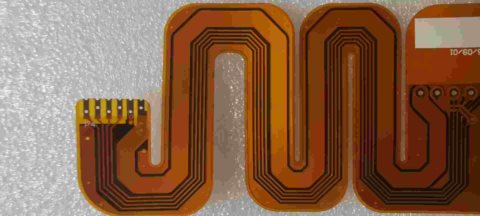
A flexible PCB is made of a thin, flexible dielectric film substrate with conductive copper traces etched or printed on one or both sides. The substrate material is usually a polyimide film like Kapton or polyester films like PET. These flex circuit materials can be bent and flexed repeatedly without damage to the copper traces. Components are soldered to the flex PCB and the flex circuit connects these components over bends and flexures in 3D space.
Flexible PCBs are ideal for many applications where rigid PCBs would fail, such as in dynamic flexing environments. Common uses for flex PCBs include:
- Wearable electronics
- Medical devices
- Robotics and UAVs
- Foldable/bendable consumer electronics
- Automotive electronics
Benefits of using flexible PCBs include:
- Can flex and bend repeatedly without damage
- Extremely lightweight and thin
- Can be folded or rolled up to save space
- Can accommodate moving or complex 3D spaces
- Vibration and impact resistant
- Easily customizable shapes and forms
With the reliability of flexible PCBs proven across many applications, the circuits can be manufactured using different methods. The three main approaches to flexible PCB printing and manufacturing are:
Laser Direct Imaging (LDI)
A laser direct images (etches) the copper traces directly onto the flex substrate material. No photolithography processes are used.
Photolithography
Using photoresist and etchant chemicals to etch the copper traces. Similar to rigid PCB fabrication.
Inkjet Printing
Inkjet technology prints the copper traces onto the substrate material with no etching required.
Next, we’ll do a deep dive into each of these flexible PCB printing methods.
Laser Direct Imaging Printing
Laser direct imaging (LDI) is one of the most advanced methods of flexible PCB printing. This technique uses a high precision laser to directly ablate or remove the unwanted copper from the flex substrate. This eliminates the need for any kind of mask, chemical etching, or complex photolithography.
How LDI Flexible PCB Printing Works
The LDI process for flex PCB printing generally follows these steps:
- The flex substrate material, usually polyimide, PET, or other polymer films, is laminated with a thin layer of copper foil on one or both sides.
- The material is loaded into a laser direct imaging system. This contains a high precision laser unit that can be digitally controlled.
- Digital artwork for the circuit traces is loaded into the LDI system as Gerber files. The laser system then meticulously traces out the artwork, vaporizing away the unwanted copper.
- The remaining copper left on the substrate forms the conductive traces for the circuit.
- Components are then soldered onto the flex PCB. Electrical tests may be conducted.
- The finished flex PCB is now ready for integration into devices and electronics.
Compared to traditional wet chemical etching, this direct laser imaging method provides many benefits:
- Extremely high resolution – traces and spaces down to 10 microns or less
- No chemicals required – environmentally friendly process
- Fast turnaround times since no etching is required
- Very accurate and precise trace geometries
- Minimal board handling so less risk of physical damage
However, LDI does require a major capital investment for the specialized laser imaging equipment. The lasers themselves are complex, delicate, and expensive devices. But the payoff is very high resolution, efficient, flexible PCB production.
LDI Flex Circuits Applications
The fine features and fast turnarounds achieved with LDI make it an excellent choice for many cutting edge flex PCB applications:
- Aerospace and defense electronics – tight tolerances required
- Wearable health monitors – precision medical devices
- Micro sensors – tiny integrated electronics
- High density interconnects – fine pitch components
- Flex antennas – microwave circuitry and traces
With laser direct imaging, intricate flexible printed circuits with trace widths below 100 micron can be achieved. LDI allows flex PCB capabilities to continue improving as lasers, positioning systems, and controller software advances.
Photolithography Flexible PCB Printing
Photolithography is the traditional process used for both rigid and flexible PCB fabrication. This well proven etching process is adapted for use with flex circuit materials. Let’s examine the step-by-step photolithography process for flex PCBs.
How Photolithography Flex Circuit Printing Works
- The base substrate material, like polyimide or PET, is laminated with copper foil on one or both sides.
- A photosensitive dry film or liquid photoresist is applied to the copper layers.
- A transparent mask is placed over the photoresist and the PCB is exposed to UV light. The mask blocks light in areas where copper should remain.
- The photoresist is developed, removing the unexposed areas of photoresist. This exposes the unwanted copper.
- The board is chemically etched to remove the exposed copper while leaving behind the desired circuit trace artwork.
- The remaining photoresist is stripped away. Components are soldered on and the flex PCB is tested.
Photolithography provides good control over trace geometries and resolution down to around 75-100 micron features. It is a well proven process used for many decades now. The main drawbacks are the multiple chemical process steps and the need to produce film masks for each unique circuit layer.
Photolithography Flex Circuits Applications
Because it is a mature, reliable fabrication technique, photolithography is used to manufacture a wide range of flex PCB applications from basic consumer electronics to high reliability systems:
- Computer peripherals – printers, disk drives
- Automotive circuitry – engine controls, sensors
- Consumer wearables – fitness bands, smart watches
- IoT devices – flexible antennas, sensors
- Medical electronics – blood glucose monitors
- Aerospace – avionics, control circuitry
With the right chemical processes and film masks, photolithography can produce durable, high performing flex circuits for mission critical electronics and systems.
Inkjet Printing Flexible PCBs
Inkjet printing takes a radically different approach to flexible PCB fabrication. Instead of etching copper away, inkjet printing uses conductive copper nanoparticle inks to directly print the circuit traces onto the substrate. This additive manufacturing process is rapid, precise, and environmentally friendly.
How Inkjet Flex Circuit Printing Works
The inkjet printing process for flex PCBs involves:
- Loading the polyimide, PET, or other flex substrate into the inkjet system.
- The proprietary conductive copper ink is loaded into the print head cartridges.
- Digital Gerber files for the circuit layout are input into the inkjet printer software.
- The print heads jet out microdroplets of the conductive ink, building up the traces.
- The ink is cured or sintered, fusing together the nanoparticles into solid copper circuits.
- Components can be soldered onto the PCB once the curing is complete.
Compared to traditional methods, inkjet printed flex PCBs offer many advantages:
- Non-contact, additive printing process
- Eliminates all the chemical waste and hazards
- Extremely rapid print times
- High resolution down to around 50 microns
- Scales well for mass production
- Well suited for rapid prototyping
The main limitation currently is the relatively high resistance of the printed traces. This restricts inkjet flex PCBs to lower frequency, lower power applications. But the technology is maturing quickly.
Inkjet Flex Circuits Applications
Inkjet printed flex circuits are ideal for:
- Consumer wearable devices
- Sensors, antennas, heaters in IoT devices
- Rapid prototyping of new flex PCB designs
- Digital health monitoring patches
- Flexible printed electronics and sensors
- Smart packaging and labels
Research into inkjet printable electronic materials is expanding the capabilities as well. Future advancements will enable printing complete flex PCB assemblies.
Flexible PCB Printing: Comparison
Laser direct imaging (LDI), traditional photolithography, and inkjet are three viable processes for flexible PCB printing and fabrication. Here is a comparison of the key characteristics:
| Method | Resolution | Chemicals | Prototyping | Notes |
|---|---|---|---|---|
| Laser Direct Imaging | 10 microns | None | Fair | Excellent resolution but slower and costly equipment |
| Photolithography | 75+ microns | Wet etching, stripping | Poor | Mature process but multiple chemical steps |
| Inkjet Printing | 50 microns | None | Excellent | Additive, rapid printing but higher trace resistance |
There are tradeoffs between resolution, cost, chemical waste, prototyping ability, and other factors for each flex PCB printing technique. Product design requirements and production parameters will determine the optimal fabrication process.
Cost Analysis of Flexible PCB Printing Methods
The costs associated with flexible PCB printing depends heavily on:
- The production volume needed
- Size of the flex circuits
- Number of layers
- Resolution and tolerances required
In general, inkjet printing has the lowest costs for low to medium production runs. The equipment is affordable and no masks or chemicals are needed. LDI provides the best accuracy and tolerances but has very high equipment costs. Photolithography sits in the middle price-wise but with higher chemical waste.
Here is an approximate cost comparison:
| Method | Setup Costs | Per Board Costs* |
|---|---|---|
| Laser Direct Imaging | $500,000+ | $100-2000 |
| Photolithography | $50,000 | $50-1500 |
| Inkjet Printing | $15,000 | $10-500 |
*Per board costs depend heavily on quantity ordered, size, layers etc.
No single method provides the perfect cost solution. Manufacturers choose the process that aligns best with the specific application requirements, budget, and business needs.
Flexible PCB Printing Challenges
While flexible PCBs provide many advantages over rigid boards, their fabrication does come with some unique challenges:
- Warping or shrinking: The polymer substrates can warp or shrink during processing. This requires advanced materials and careful process control.
- Registration: Aligning layers, inkjet passes, and laser scans can be difficult on flexing, moving material. Automated optical registration is usually required.
- Fine features: Flexible substrates can make it harder to achieve very fine circuit traces and spaces versus FR-4 material.
- Soldering: The thin, flexible boards can make soldering components tricky without warping or damaging the traces.
- Costs: Especially for lower volume orders, flex PCB costs are generally higher than rigid PCB fabrication.
However, the benefits of flexible printed circuits outweigh these challenges in most cases. And improvements in flex PCB printing technology continues to overcome issues.
The Future of Flexible PCB Printing
Printed electronics and flexible PCB manufacturing technology continues advancing rapidly. Here are some exciting areas to look forward to:
- Inkjet printing improvements – Better conductivity, embedded passives, 3D printing
- LDI advancements – Faster speeds, lower costs, embedded component assembly
- Nanotechnology applications – Printed transistors, batteries, sensors, antennas
- Biocompatible materials – Implantable medical devices, wearable monitors
- Hybrid processes – Combining inkjet, photolithography, LDI, etc.
- High frequency, high speed flex – > 10 GHz traces
- Encapsulation/packaging – Protecting bare flex PCBs
The applications for printed flexible circuit boards are nearly endless. Along with the PCB fabrication methods, new inks, materials, and printing technologies will expand possibilities even further in the future.
Conclusion
Flexible printed circuit boards enable electronics and devices that would be impossible with rigid PCBs. As demand grows, laser direct imaging, photolithography, and inkjet printing have all proven to be viable fabrication techniques – each with their own pros and cons. Engineers must weigh the tradeoffs between costs, chemical waste, turnaround times, resolution needs and other factors when selecting the optimal flex PCB printing process. With further development, flexible PCBs will continue improving our electronics and products.
Flexible PCB Printing Frequently Asked Questions
Here are some common FAQs about flexible PCB printing methods:
Q1: What is the minimum trace width and space achievable with each printing method?
A: The minimum feature sizes are approximately:
- Laser direct imaging: 10 microns
- Photolithography: 75-100 microns
- Inkjet printing: 50 microns
Laser direct imaging can achieve the finest resolution. Inkjet is nearly as good while photolithography has somewhat larger minimum features.
Q2: Can components be assembled directly onto printed flexible PCBs?
A: Yes, surface mount components can be soldered onto all the flex PCBs after printing. Photolithography PCBs can also support through hole components. Extra care must be taken during assembly to not damage the flexible boards.
Q3: How many flex PCB layers can be produced?
A: All the methods can support double sided flex PCBs. Photolithography and laser direct imaging can routinely produce 4-6 layer (or more) multilayer flex circuits as well. Inkjet printed circuits are typically single or double sided.
Q4: Can these processes make both rigid and flex PCBs?
A: Photolithography uses the same equipment and processes for both rigid and flex PCB fabrication. Laser direct imaging and inkjet printing are optimized for flexible substrates.
Q5: How environmentally friendly are these flex PCB printing methods?
A: Inkjet printing is the most green since no chemicals are used. Photolithography uses significant hazardous chemicals. LDI uses no chemicals but higher power lasers.
In summary, each flexible PCB printing technology has advantages and tradeoffs. Product requirements and production parameters will determine the best fabrication process for a given application.


Leave a Reply