What is a Gerber File?
A Gerber file is a standard file format used in the printed circuit board (PCB) industry to describe the printed circuit board images: copper layers, solder mask, legend, drill holes, etc. It is a vector image file format developed by Ucamco, containing all the necessary information for PCB fabrication and assembly. Gerber files are also known as Gerber Image files or Gerber Format Plot files with file extensions .gbr or .art.
Gerber files are essential for PCB manufacturing as they provide precise information about the PCB design to the fabrication house. The fabricator uses these files to create the photomasks, stencils, and drilling templates necessary for manufacturing the PCB.
Gerber File Structure
A Gerber file consists of a sequence of commands that describe the various features of a PCB layer. These commands include:
- Aperture definitions: Define the shapes and sizes of the pads, tracks, and other features.
- Aperture selections: Specify which aperture to use for the following plot commands.
- Plot commands: Describe the actual image (tracks, pads, etc.) using the selected aperture.
- Coordinate commands: Specify the position of the aperture on the PCB.
- Miscellaneous commands: Include file attributes, comments, etc.
Here’s an example of a simple Gerber file:
G04 Gerber File Example*
%FSLAX25Y25*%
%MOMM*%
%ADD10C,0.1*%
D10*
X100000Y100000D02*
X200000Y200000D01*
M02*
In this example:
– G04 is a comment.
– %FSLAX25Y25% sets the format specification to 2.5 integer and 2.5 decimal places.
– %MOMM% sets the unit to millimeters.
– %ADD10C,0.1% defines an aperture with ID 10, a circular shape, and a diameter of 0.1mm.
– D10 selects the aperture with ID 10.
– X100000Y100000D02 moves the aperture to the coordinate (10.0000, 10.0000) without drawing.
– X200000Y200000D01 draws a line to the coordinate (20.0000, 20.0000).
– M02* indicates the end of the file.
Gerber File Types
A complete PCB design consists of several Gerber files, each representing a different layer or aspect of the PCB. The most common Gerber file types include:
- Copper layers (GTL, G1L, G2L, etc.): Describe the copper traces and pads on each layer of the PCB.
- Solder mask layers (GTS, GBS): Define the areas where solder mask should be applied to protect the copper traces.
- Silkscreen layers (GTO, GBO): Contain the text and graphics printed on the PCB for component placement and identification.
- Solder paste layers (GTP, GBP): Specify the areas where solder paste should be applied for surface mount components.
- Drill files (TXT, DRL): Contain information about the size and location of drilled holes on the PCB.

Creating Gerber Files
Most PCB design software, such as Altium Designer, KiCad, and Eagle, can generate Gerber files from the PCB design. The process usually involves selecting the desired layers, setting the output parameters (e.g., unit, format, etc.), and choosing a destination folder for the generated files.
Here are some general steps to create Gerber files in PCB design software:
- Complete your PCB design, ensuring that all layers are correctly defined and named.
- Open the Gerber file generation tool in your PCB design software.
- Select the layers you want to include in the Gerber files (copper, solder mask, silkscreen, etc.).
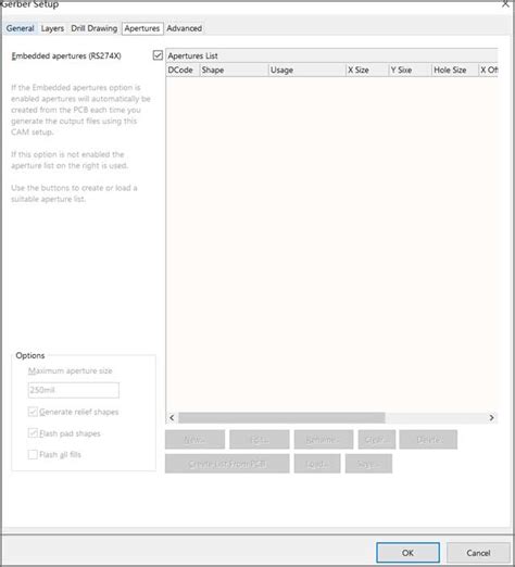
- Set the output parameters, such as unit (usually millimeters), format (e.g., 2.5), and aperture list type (embedded or separate file).
- Choose a destination folder for the generated Gerber files.
- Generate the Gerber files and review them using a Gerber viewer to ensure accuracy.
Gerber File Generation Settings
When generating Gerber files, it’s essential to choose the appropriate settings to ensure compatibility with the fabrication house and avoid manufacturing issues. Some key settings to consider include:
- Unit: Most fabrication houses prefer millimeters (mm) as the unit for Gerber files.
- Format: The most common format is 2.5 (2 integer digits and 5 decimal digits), but some fabricators may require other formats like 2.4 or 2.6.
- Aperture list: An embedded aperture list is preferred, as it keeps all the necessary information within the Gerber file itself.
- Coordinate format: Absolute coordinates are more common and easier to interpret than incremental coordinates.
- Drill file format: Most fabricators prefer ASCII format (TXT) for drill files, but some may also accept Excellon format (DRL).
It’s always a good idea to consult with your chosen fabrication house for their specific Gerber file requirements and settings.

Reviewing Gerber Files
Before sending Gerber files to a fabrication house, it’s crucial to review them for accuracy and completeness. This helps to catch any errors or discrepancies early in the process, saving time and money on potential revisions.
There are several Gerber viewer software available, both online and offline, that allow you to visualize and analyze Gerber files. Some popular options include:
- Gerbv: A free, open-source Gerber viewer for Linux, macOS, and Windows.
- ViewMate: A free online Gerber viewer provided by PCBWay.
- CAM350: A professional PCB CAM software with advanced Gerber viewing and editing capabilities.
When reviewing Gerber files, look for the following:
- Layer alignment: Ensure that all layers are correctly aligned and there are no unintended offsets.
- Aperture definitions: Check that all apertures are correctly defined and match the intended design.
- Trace and pad sizes: Verify that the trace widths and pad sizes meet the design requirements and manufacturing constraints.
- Clearances: Ensure that there are no violations of the minimum clearance between traces, pads, and other features.
- Drill holes: Check that all drill holes are correctly positioned and sized.
Common Gerber File Issues
Some common issues to watch out for when reviewing Gerber files include:
- Missing layers: Ensure that all necessary layers (copper, solder mask, silkscreen, etc.) are included in the Gerber file set.
- Incorrect units: Verify that the Gerber files use the correct unit (usually millimeters) and format (e.g., 2.5).
- Overlapping features: Check for any overlapping traces, pads, or other features that may cause short circuits or manufacturing issues.
- Insufficient clearances: Ensure that the design maintains the minimum required clearances between features to avoid manufacturing problems.
- Incorrect aperture sizes: Verify that the aperture sizes match the intended design and are within the manufacturing constraints.
By carefully reviewing Gerber files before submitting them to a fabrication house, you can minimize the risk of costly mistakes and ensure a smooth PCB manufacturing process.

Gerber File Best Practices
To ensure the best results when working with Gerber files, follow these best practices:
- Use a consistent naming convention for your Gerber files, including the PCB name, layer type, and version number (e.g., PCB_Name_Copper_Top_v1.0.gbr).
- Always include a readme file with your Gerber files that describes the PCB, lists the included files, and specifies any special requirements or instructions.
- Use a Gerber viewer to review your files before submitting them to the fabrication house to catch any errors or discrepancies early.
- Communicate with your fabrication house to understand their specific Gerber file requirements and settings.
- Keep your Gerber files organized and version-controlled to avoid confusion and ensure traceability.
- When in doubt, consult with experienced PCB designers or your fabrication house for guidance and best practices.
Gerber File FAQs
- What is the difference between Gerber files and ODB++ files?
-
Gerber files are a standard file format for describing PCB images, while ODB++ (Open Database++) is a more comprehensive PCB data exchange format that includes Gerber data along with additional information such as component placement, netlist, and design rules.
-
Can I view Gerber files without specialized software?
-
While it’s possible to open Gerber files in a text editor, it’s not recommended as the files are difficult to interpret without proper visualization. It’s best to use a dedicated Gerber viewer or PCB CAM software to properly view and analyze Gerber files.
-
What should I do if my fabrication house reports issues with my Gerber files?
-
If your fabrication house reports issues with your Gerber files, first try to understand the specific problem they have identified. Review your files using a Gerber viewer to see if you can spot the issue. If necessary, go back to your PCB design software, make the required changes, and regenerate the Gerber files. Always communicate with your fabrication house to resolve any issues and ensure a smooth manufacturing process.
-
Can I edit Gerber files directly?
-
While some PCB CAM software allows for limited editing of Gerber files, it’s generally not recommended to edit them directly. Instead, make any necessary changes in your PCB design software and regenerate the Gerber files to ensure consistency and avoid introducing errors.
-
How do I choose the right fabrication house for my PCB project?
- When choosing a fabrication house, consider factors such as their experience, capabilities, quality control processes, and customer support. Look for reviews and recommendations from other PCB designers, and don’t hesitate to ask questions about their Gerber file requirements, manufacturing constraints, and turnaround times. Establishing a good relationship with a reliable fabrication house can greatly contribute to the success of your PCB projects.
Conclusion
Gerber files are essential for PCB manufacturing, providing the necessary information for fabrication houses to produce high-quality PCBs. By understanding Gerber file structure, types, and best practices, PCB designers can ensure that their designs are accurately translated into physical boards.
When working with Gerber files, remember to:
- Generate Gerber files with the appropriate settings and layers.
- Review Gerber files using a dedicated viewer to catch errors and discrepancies.
- Communicate with your fabrication house to understand their specific requirements.
- Follow best practices for naming, organizing, and version-controlling your Gerber files.
By mastering Gerber files, PCB designers can streamline the manufacturing process, reduce the risk of errors, and ultimately create successful PCB projects.


Leave a Reply