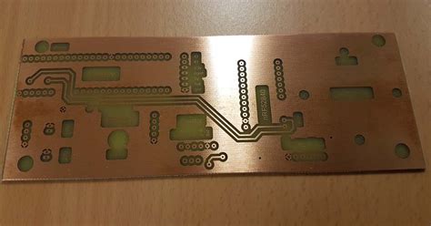
What is PCB Etching?
PCB etching is a critical process in the manufacturing of printed circuit boards (PCBs) where unwanted copper is removed from the surface of the board, leaving behind the desired copper traces that form the electrical connections. Etching is typically performed using chemical solutions that selectively dissolve the copper while leaving the protective mask intact.
Types of PCB Etching
There are two main types of PCB etching:
- Subtractive etching
- Additive etching
In subtractive etching, a layer of copper is first laminated onto the entire surface of the PCB substrate. A protective mask is then applied on top of the copper in the pattern of the desired traces. The board is exposed to an etchant solution which removes the unmasked copper, leaving behind the traces. Subtractive etching is the most common method used in PCB production.
Additive etching, also known as pattern plating, starts with a Bare PCB substrate. A thin layer of copper is electrolessly deposited only on the areas where traces are desired. Additional copper is then electroplated on top to build up the thickness of the traces. Since copper is only added where needed, additive etching eliminates the material waste of the subtractive process. However, it is more expensive and mainly used for special applications.
The Inner Layer Etching Process
Preparing the Inner Layer
PCBs are built up layer by layer. The inner layers contain the interconnections between components on different layers. Before etching, the inner layer must first be prepared:
- The inner layer starts as a thin, copper-clad laminate
- A photoresist (light-sensitive polymer) is applied on both sides of the laminate
- The photoresist is exposed to light through a photomask containing the trace pattern
- The photoresist is developed, hardening the exposed areas
- The unexposed photoresist is stripped away, leaving behind a protective mask over the traces
- The panel is now ready for etching
Etching the Inner Layer
With the protective mask in place, the inner layer panel is now put through the etching process:
- The panel is immersed in an etchant solution, typically cupric chloride or ammonium persulfate
- The etchant chemically reacts with and dissolves the unmasked copper
- The panel is removed from the etchant once all the unmasked copper is gone, typically 1-2 minutes
- The panel is rinsed to remove any remaining etchant
- The protective mask is stripped off, revealing the etched copper traces
- The panel is inspected for proper etching and any defects
Etchant Chemistry
The two most common etchants used for inner layers are:
| Etchant | Composition | Advantages | Disadvantages |
|---|---|---|---|
| Cupric Chloride | CuCl2 + HCl | Fast etching, can be regenerated | Corrosive, disposal issues |
| Ammonium Persulfate | (NH4)2S2O8 | Clean, non-corrosive | Slower etching, one-time use |
Cupric chloride works by oxidizing the copper, forming cuprous chloride (CuCl) which is soluble in the etchant. The reaction regenerates cupric chloride, allowing it to continue etching. Hydrochloric acid (HCl) is added to regenerate the cupric chloride and prevent the precipitation of cuprous chloride.
Ammonium persulfate directly oxidizes the copper to form copper sulfate, which remains dissolved in solution. The persulfate is consumed in the reaction and cannot be regenerated, so the etchant must be replaced once it is exhausted.
Etchant Control
For an optimal etch, the etchant must be carefully controlled:
-
Temperature: Higher temperature accelerates chemical reaction and etching rate. Typical range is 110-130°F (43-54°C).
-
pH: Acidic pH is required for proper etching. Cupric chloride is maintained at a pH of 8.0-8.5 by HCl addition. Ammonium persulfate naturally gives a pH around 2.
-
Specific gravity (SG): Measures etchant concentration. Cupric chloride is kept around 1.26 g/mL SG, ammonium persulfate at 1.33 g/mL SG.
-
Oxidation-Reduction Potential (ORP): Indicates the oxidizing power of the etchant. Cupric chloride is controlled at 525-575 mV vs. Ag/AgCl reference electrode.
-
Dissolved copper: As etching proceeds, copper builds up in the etchant. Excessive copper slows down etching. Cupric chloride can be electrolytically regenerated to remove copper.

Multilayer PCB Considerations
Etching the inner layers is a key step in the Multilayer PCB Fabrication process. There are several important considerations:
Registration
The etched inner layer traces must align precisely with the drilled via holes and outer layer traces. Fiducial marks, which are round copper pads etched in the corners of the panel, help align the layers during lamination and drilling. The layer-to-layer registration must typically be within ±3 mils (±76 μm).
Trace Width and Spacing
The minimum trace width and spacing that can be etched depends on the capabilities of the PCB manufacturer. Typical minimums are around 3-4 mils (76-102 μm) for standard PCBs. More advanced processes can achieve 1-2 mils (25-51 μm).
Etch Factor
The etchant dissolves the copper not just downward but also sideways under the mask. This results in the trace width being narrower at the top surface than at the bottom, producing a trapezoidal cross-section. The ratio of undercut to etch depth is called the etch factor, which is typically around 1:4 to 1:3. The etch factor must be compensated for when designing the trace widths and spaces.
Copper Weight
The starting copper weight (thickness) of the inner layer laminate is typically ½ oz or 1 oz per square foot, which corresponds to 18 μm or 35 μm thickness respectively. A thicker copper requires a longer etch time. The etched traces will be slightly thinner than the starting copper weight due to sidewall etch.

FAQ
What is the most common etchant used for PCB inner layers?
Cupric chloride (CuCl2) and ammonium persulfate ((NH4)2S2O8) are the two most widely used etchants for inner layer etching. Cupric chloride is faster and can be regenerated, while ammonium persulfate is cleaner and less corrosive.
What is the purpose of etching inner layers in PCB fabrication?
Etching the inner layers creates the copper interconnect traces that form the electrical pathways between different layers of the PCB. The traces on each inner layer must be precisely etched in order to align with the vias and component pads drilled through the board later in the fabrication process.
How thick are the copper traces on a typical inner layer?
The most common starting copper weights for inner layer laminates are ½ oz and 1 oz per square foot, which correspond to 18 μm and 35 μm copper thickness respectively. After etching, the traces will be slightly thinner due to lateral etching under the photoresist mask.
What is the minimum trace width and spacing achievable with inner layer etching?
For a standard PCB fabrication process, the minimum etched trace width and spacing is typically around 3-4 mils (76-102 μm). More advanced processes can achieve 2 mils (51 μm) and below. The achievable minimums depend on the photoresist resolution, etching chemistry, and other factors specific to the PCB manufacturer.
How are the inner layers aligned to each other in the final PCB?
Fiducial marks are etched on the inner layers along with the traces. These are typically round copper pads placed in the corners of the panel. The fiducials are used to align the layers during lamination and drilling. Layer-to-layer registration is typically controlled to within ±3 mil (76 μm) or better.


Leave a Reply