What is a Bare PCB?
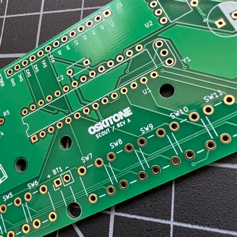
A bare printed circuit board, also known as a blank PCB, is the foundation of any electronic device. It is a flat, rigid board made of insulating material, typically fiberglass or composite epoxy, with conductive pathways etched onto its surface. These pathways, called traces, connect various components such as resistors, capacitors, and integrated circuits to create a functional electronic circuit.
Bare PCBs are the starting point for assembling electronic devices. They provide a stable platform for mounting components and ensure proper electrical connections between them. The quality and design of the bare PCB greatly influence the performance, reliability, and longevity of the final electronic product.
Types of Bare PCBs
There are several types of bare PCBs, each with its own unique characteristics and applications:
-
Single-sided PCB: These PCBs have conductive traces on only one side of the board. They are the simplest and most cost-effective option, suitable for low-complexity circuits.
-
Double-sided PCB: These PCBs have conductive traces on both sides of the board, allowing for more complex designs and higher component density. The two sides are connected using through-hole vias.
-
Multi-layer PCB: These PCBs consist of multiple layers of insulating material and conductive traces. They offer the highest level of complexity and are used in advanced electronic devices that require high-speed signal processing and dense component placement.
-
Flexible PCB: These PCBs are made of flexible insulating material, allowing them to bend and conform to various shapes. They are ideal for applications where space is limited or where the PCB needs to fit into a specific form factor.
-
Rigid-Flex PCB: These PCBs combine the benefits of both rigid and flexible PCBs. They consist of rigid sections connected by flexible sections, enabling complex 3D designs and improved reliability in applications that require both stability and flexibility.
| PCB Type | Layers | Complexity | Cost | Applications |
|---|---|---|---|---|
| Single-sided | 1 | Low | Low | Simple circuits, low-power devices |
| Double-sided | 2 | Medium | Medium | General-purpose electronics |
| Multi-layer | 3+ | High | High | Advanced electronics, high-speed devices |
| Flexible | 1-2 | Low-Medium | Medium-High | Wearables, compact devices |
| Rigid-Flex | 2+ | High | High | Complex 3D designs, aerospace, military |
PCB Manufacturing Process
The manufacturing process of bare PCBs involves several key steps:
1. PCB Design
The first step in creating a bare PCB is designing the circuit layout using specialized software called Electronic Design Automation (EDA) tools. The design includes the placement of components, routing of traces, and the creation of solder masks and silkscreen layers.
2. PCB Fabrication
Once the design is finalized, the PCB fabrication process begins:
-
Substrate preparation: The insulating substrate, usually fiberglass or composite epoxy, is cut to the desired size and thickness.
-
Copper lamination: A thin layer of copper foil is laminated onto the substrate using heat and pressure.
-
Photoresist application: A light-sensitive photoresist is applied to the copper layer.
-
Exposure and development: The photoresist is exposed to UV light through a photomask, which transfers the circuit pattern onto the photoresist. The unexposed areas are then removed during the development process.
-
Etching: The exposed copper is removed using a chemical etching process, leaving only the desired conductive traces.
-
Drilling: Holes are drilled through the board to accommodate through-hole components and vias.
-
Solder mask application: A protective solder mask is applied to the board, covering the areas where soldering is not required.
-
Silkscreen printing: Text, logos, and component identifiers are printed onto the board using silkscreen printing.
-
Surface finish: A surface finish, such as HASL (Hot Air Solder Leveling), ENIG (Electroless Nickel Immersion Gold), or OSP (Organic Solderability Preservative), is applied to the exposed copper traces to prevent oxidation and enhance solderability.
3. Quality Control
Throughout the manufacturing process, strict quality control measures are implemented to ensure the bare PCBs meet the required specifications. These measures include:
- Visual inspection
- Automated Optical Inspection (AOI)
- Electrical testing
- Dimensional verification

Bare PCB Design Considerations
When designing a bare PCB, several key factors must be considered to ensure optimal performance and manufacturability:
1. Material Selection
The choice of PCB material depends on the specific application requirements, such as temperature range, dielectric constant, and thermal conductivity. Common materials include:
- FR-4: A glass-reinforced epoxy laminate, widely used for general-purpose applications.
- High-Tg FR-4: A variant of FR-4 with improved thermal stability, suitable for high-temperature applications.
- Polyimide: A flexible material with excellent thermal and chemical resistance, used in flexible and rigid-flex PCBs.
- PTFE (Teflon): A low-dielectric-constant material with excellent high-frequency performance, used in RF and microwave applications.
2. Trace Width and Spacing
The width and spacing of conductive traces on a bare PCB must be carefully designed to ensure proper signal integrity and manufacturability. Factors to consider include:
- Current-carrying capacity: Wider traces are needed for high-current signals to prevent overheating and voltage drop.
- Impedance control: Trace width and spacing affect the characteristic impedance of the signal traces, which is critical for high-speed digital signals.
- Manufacturing constraints: Minimum trace width and spacing are limited by the PCB fabrication process and the chosen copper weight.
3. Via Design
Vias are conductive pathways that connect different layers of a PCB. Proper via design is crucial for signal integrity and manufacturability. Considerations include:
- Via size: The diameter of the via drill hole and the annular ring must be sufficient to ensure reliable connections and manufacturability.
- Via type: Through-hole vias, blind vias, and buried vias are used depending on the PCB layer structure and design requirements.
- Via stitching: Adding additional vias along a signal path can help reduce inductance and improve signal integrity.
4. Component Placement
The placement of components on a bare PCB affects signal integrity, thermal management, and manufacturability. Guidelines for component placement include:
- Grouping related components together to minimize signal path lengths and reduce crosstalk.
- Placing heat-generating components away from temperature-sensitive components and providing adequate thermal relief.
- Ensuring sufficient clearance between components for assembly and rework.
- Orienting components to facilitate automated assembly processes, such as pick-and-place and wave soldering.

Advantages of Using Bare PCBs
Using bare PCBs offers several advantages over other electronic circuit construction methods:
-
Consistency and reliability: PCBs provide a consistent and reliable platform for electronic circuits, ensuring proper connections and reducing the risk of errors.
-
Miniaturization: PCBs enable the creation of compact and high-density electronic devices, allowing for smaller and more portable end products.
-
Automated assembly: Bare PCBs are designed for automated assembly processes, such as pick-and-place and wave soldering, which greatly reduces manufacturing time and costs.
-
Scalability: PCBs can be easily mass-produced, making them ideal for large-scale production runs and reducing per-unit costs.
-
Customization: PCBs can be customized to meet specific design requirements, such as unique form factors, high-speed signal processing, or environmental resistance.

Bare PCB Testing and Inspection
To ensure the quality and reliability of bare PCBs, various testing and inspection methods are employed:
-
Visual inspection: A manual or automated visual inspection checks for obvious defects, such as missing traces, short circuits, or damaged components.
-
Automated Optical Inspection (AOI): AOI systems use high-resolution cameras and image processing algorithms to detect surface-level defects, such as solder bridges, missing components, or incorrect component placement.
-
X-ray inspection: X-ray imaging is used to detect internal defects, such as voids in solder joints or misaligned through-hole components.
-
Electrical testing: Various electrical tests, such as continuity testing, insulation resistance testing, and high-potential (hipot) testing, are performed to verify the electrical integrity of the PCB and ensure compliance with safety standards.
-
Functional testing: The bare PCB is powered up and tested under real-world operating conditions to verify its functionality and performance.
Bare PCB Packaging and Storage
Proper packaging and storage of bare PCBs are essential to maintain their quality and prevent damage during transportation and handling:
-
ESD protection: Bare PCBs are susceptible to electrostatic discharge (ESD) damage, so they must be packaged in ESD-safe materials, such as antistatic bags or conductive foam.
-
Moisture protection: Exposure to moisture can lead to corrosion and delamination of the PCB. Moisture-barrier bags with desiccants are used to protect the PCBs during storage and transportation.
-
Physical protection: PCBs should be packaged in sturdy boxes or containers to prevent physical damage during handling and shipping.
-
Environmental control: PCBs should be stored in a cool, dry environment with controlled humidity to prevent moisture absorption and thermal stress.
Future Trends in Bare PCB Technology
As electronic devices continue to evolve, so do the technologies and trends in bare PCB manufacturing:
-
Miniaturization: The demand for smaller and more compact electronic devices is driving the development of advanced PCB technologies, such as high-density interconnect (HDI) and embedded component PCBs.
-
High-speed materials: The increasing need for high-speed data transmission is leading to the adoption of low-loss, high-frequency PCB materials, such as PTFE and hydrocarbon ceramic laminates.
-
Additive manufacturing: 3D printing technologies are being explored for PCB fabrication, enabling the creation of complex 3D structures and reducing waste material.
-
Environmental sustainability: There is a growing emphasis on environmentally friendly PCB materials and manufacturing processes, such as halogen-free laminates and lead-free soldering.
-
Intelligent PCBs: The integration of sensors, processors, and communication modules directly onto PCBs is enabling the development of intelligent and connected electronic devices.
FAQ
-
What is the difference between a bare PCB and an assembled PCB?
A bare PCB is a printed circuit board without any components mounted on it, while an assembled PCB has components soldered onto the board, ready for use in an electronic device. -
Can I design my own bare PCB?
Yes, you can design your own bare PCB using Electronic Design Automation (EDA) software. However, it is essential to have a good understanding of PCB design principles and manufacturing constraints to ensure a successful outcome. -
How do I choose the right bare PCB material for my application?
The choice of PCB material depends on factors such as the operating temperature range, dielectric constant, thermal conductivity, and mechanical requirements of your application. Consult with a PCB manufacturer or materials expert to select the most suitable material for your needs. -
What is the minimum trace width and spacing achievable on a bare PCB?
The minimum trace width and spacing depend on the PCB fabrication process and the chosen copper weight. Typical minimum trace widths range from 3 to 6 mils (0.075 to 0.15 mm), while minimum spacing ranges from 3 to 8 mils (0.075 to 0.2 mm). However, advanced PCB technologies, such as HDI, can achieve even smaller dimensions. -
How long does it take to manufacture a bare PCB?
The manufacturing time for a bare PCB depends on various factors, such as the complexity of the design, the chosen fabrication process, and the workload of the PCB manufacturer. Typical lead times range from a few days to several weeks, with expedited services available for urgent projects.
Conclusion
Bare printed circuit boards are the foundation of modern electronic devices, providing a reliable and efficient platform for mounting components and creating complex circuits. Understanding the types of bare PCBs, their manufacturing process, design considerations, and testing methods is crucial for designing and producing high-quality electronic products.
As technology advances, bare PCB technology continues to evolve, with trends such as miniaturization, high-speed materials, additive manufacturing, environmental sustainability, and intelligent PCBs shaping the future of the industry.
By staying informed about the latest developments in bare PCB technology and working closely with experienced PCB manufacturers, designers and engineers can create innovative and reliable electronic devices that meet the ever-growing demands of the market.


Leave a Reply