Introduction to Fly Buck Converters and PCB layout
Fly buck converters, also known as isolated buck converters, are widely used in power electronics to step down high voltages to lower levels while providing electrical isolation between the input and output. These converters play a crucial role in various applications, including telecommunications, industrial control systems, and consumer electronics. To ensure optimal performance and reliability of fly buck converters, proper PCB layout techniques are essential.
In this article, we will explore the key considerations and best practices for designing PCB layouts for fly buck converters. We will discuss the importance of component placement, trace routing, grounding, and thermal management. By following these guidelines, you can minimize electromagnetic interference (EMI), reduce power losses, and enhance the overall efficiency and stability of your fly buck converter design.
Understanding the Basics of Fly Buck Converters
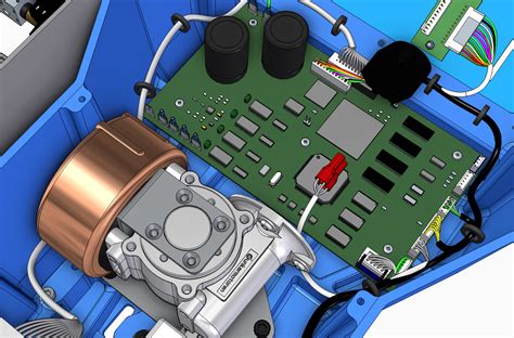
Before diving into PCB layout tips, let’s briefly review the fundamentals of fly buck converters. A fly buck converter consists of a primary side and a secondary side, separated by a transformer. The primary side includes a switch (usually a MOSFET), a transformer primary winding, and a control circuit. The secondary side comprises a transformer secondary winding, rectifier diodes, an output filter (inductor and capacitor), and a load.
The working principle of a fly buck converter involves turning the primary side switch on and off at a high frequency. When the switch is on, energy is stored in the transformer’s magnetic field. When the switch turns off, the stored energy is transferred to the secondary side, where it is rectified and filtered to provide a regulated DC output voltage.

Key Considerations for Fly Buck Converter PCB Layout
Component Placement
Proper component placement is crucial for minimizing parasitic inductances and capacitances, which can lead to increased losses and EMI. Here are some guidelines for component placement:
- Place the primary side components (switch, transformer primary winding, and control circuit) close together to minimize loop areas and reduce parasitic inductances.
- Position the switch and its associated components (e.g., gate resistor and snubber) as close as possible to the transformer primary winding to minimize the primary loop area.
- Place the secondary side components (rectifier diodes, output filter, and load) close to the transformer secondary winding to minimize the secondary loop area and reduce losses.
- Keep sensitive control circuitry away from high-current paths and noisy components to avoid interference.
Trace Routing
Trace routing plays a significant role in minimizing EMI and reducing power losses. Consider the following tips:
- Use wide traces for high-current paths to minimize resistive losses and improve current carrying capacity.
- Keep trace lengths as short as possible to reduce parasitic inductances and resistances.
- Route power and ground traces on separate layers to minimize loop areas and reduce EMI.
- Use a star ground configuration, where all ground connections meet at a single point, to avoid ground loops and minimize ground bounce.
- Avoid routing sensitive signal traces parallel to high-current paths to prevent crosstalk and interference.
Grounding
Proper grounding is essential for minimizing EMI and ensuring stable operation of the fly buck converter. Here are some grounding techniques to consider:
- Use a solid ground plane on one or more layers of the PCB to provide a low-impedance return path for high-frequency currents.
- Connect the primary and secondary ground planes using a single point or a small


Leave a Reply