Introduction to PCB 3D Design
Printed Circuit Board (PCB) design has evolved significantly over the years, and one of the most notable advancements is the incorporation of 3D functions. PCB 3D design has revolutionized the way engineers and designers approach the creation of electronic devices, offering a range of benefits that were previously unattainable with traditional 2D design methods.
In this article, we will explore the reasons why PCB design has embraced 3D functions, the advantages they offer, and how they have transformed the electronics industry. We will also discuss the tools and techniques used in PCB 3D design, as well as the challenges and future prospects of this technology.
The Need for PCB 3D Design
As electronic devices become increasingly complex and compact, the demand for more sophisticated PCB designs has grown. Traditional 2D design methods, while still useful for simple circuits, have limitations when it comes to designing high-density, multi-layered boards. This is where PCB 3D design comes into play.
Advantages of PCB 3D Design
-
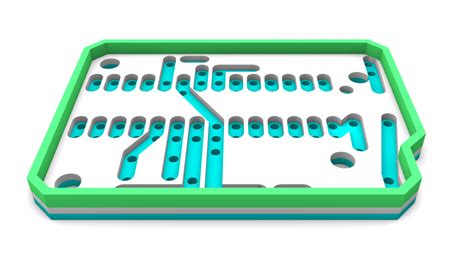
Improved Visualization: One of the primary advantages of PCB 3D design is the enhanced visualization it provides. With 3D models, designers can view the PCB from any angle, zoom in and out, and even see through layers. This allows for a better understanding of the board’s layout, component placement, and potential issues.
-
Enhanced Collaboration: PCB 3D design facilitates collaboration among team members, as the 3D models can be easily shared and discussed. This is particularly useful for large, complex projects that involve multiple stakeholders, such as engineers, designers, and manufacturers.
-
Increased Accuracy: With PCB 3D design, designers can create highly accurate models of the board, taking into account factors such as component dimensions, clearances, and thermal considerations. This reduces the likelihood of errors and ensures that the final product meets the desired specifications.
-
Faster Prototyping: 3D design allows for faster prototyping, as the models can be easily modified and tested virtually before physical prototypes are created. This saves time and resources, as fewer iterations are required to arrive at the final design.

Tools and Techniques for PCB 3D Design
To fully leverage the benefits of PCB 3D design, engineers and designers rely on a range of tools and techniques. These include:
3D CAD Software
There are several 3D CAD (Computer-Aided Design) software packages available specifically for PCB design. These tools allow designers to create detailed 3D models of the board, including components, traces, and vias. Some popular PCB 3D CAD software include:
- Autodesk EAGLE
- Altium Designer
- KiCad
- Mentor Graphics PADS
| Software | Key Features |
|---|---|
| Autodesk EAGLE | – User-friendly interface – Extensive component libraries – Integration with Fusion 360 for mechanical design |
| Altium Designer | – Powerful 3D modeling capabilities – Real-time design rule checking – Collaboration tools for team projects |
| KiCad | – Open-source and free to use – Support for multi-layered boards – Integration with FreeCAD for mechanical design |
| Mentor Graphics PADS | – Advanced simulation and analysis tools – Automated design rule checking – Support for high-speed and RF designs |
3D Printing
3D printing has become an increasingly popular technique for prototyping PCBs. By 3D printing the board, designers can quickly and easily create physical models to test fit, form, and function. This is particularly useful for boards with complex geometries or unconventional shapes.
Virtual Reality (VR) and Augmented Reality (AR)
VR and AR technologies are also finding applications in PCB 3D design. By using VR headsets or AR devices, designers can immerse themselves in the 3D model of the board, allowing for a more intuitive and interactive design experience. This can help identify potential issues and optimize the layout more efficiently.

Challenges and Future Prospects
While PCB 3D design offers numerous benefits, it also presents some challenges. One of the main challenges is the learning curve associated with 3D CAD software, which can be steep for designers accustomed to traditional 2D design methods. Additionally, the cost of 3D CAD software and hardware can be a barrier for some companies, particularly smaller businesses.
Despite these challenges, the future of PCB 3D design looks bright. As the technology continues to evolve and become more accessible, it is expected to become an increasingly essential tool for electronics design. Some potential future developments include:
- Integration of artificial intelligence (AI) and machine learning (ML) to automate and optimize the design process
- Increased use of VR and AR for immersive design experiences
- Development of more advanced materials and manufacturing techniques for 3D-Printed PCBs
- Greater adoption of 3D design in industries beyond electronics, such as aerospace and automotive

Frequently Asked Questions (FAQ)
-
Q: What are the main benefits of using 3D functions in PCB design?
A: The main benefits of using 3D functions in PCB design include improved visualization, enhanced collaboration, increased accuracy, and faster prototyping. -
Q: Do I need special software for PCB 3D design?
A: Yes, you will need 3D CAD software specifically designed for PCB design. Some popular options include Autodesk EAGLE, Altium Designer, KiCad, and Mentor Graphics PADS. -
Q: Is 3D printing a viable option for prototyping PCBs?
A: Yes, 3D printing is becoming increasingly popular for prototyping PCBs, especially for boards with complex geometries or unconventional shapes. -
Q: Are VR and AR technologies used in PCB 3D design?
A: Yes, VR and AR technologies are finding applications in PCB 3D design, allowing for a more intuitive and interactive design experience. -
Q: What are some potential future developments in PCB 3D design?
A: Some potential future developments in PCB 3D design include the integration of AI and ML, increased use of VR and AR, development of advanced materials and manufacturing techniques for 3D-printed PCBs, and greater adoption of 3D design in industries beyond electronics.
Conclusion
PCB 3D design has revolutionized the way electronic devices are created, offering a range of benefits that were previously unattainable with traditional 2D design methods. By leveraging 3D CAD software, 3D printing, and VR/AR technologies, engineers and designers can create highly accurate, visually stunning, and efficiently manufactured PCBs.
As the technology continues to evolve and become more accessible, it is expected to play an increasingly crucial role in the electronics industry and beyond. With the potential for AI integration, immersive design experiences, and advanced manufacturing techniques, the future of PCB 3D design is both exciting and promising.


Leave a Reply