What is a 3D-Printed PCB?
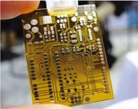
A 3D-printed PCB, also known as a 3D-printed circuit board or a 3D-printed electronic circuit, is a functional printed circuit board created using additive manufacturing techniques. Unlike traditional PCB manufacturing methods that involve subtractive processes like etching and drilling, 3D printing allows for the direct deposition of conductive and insulating materials to form the desired circuit pattern.
The process of creating a 3D-printed PCB involves using specialized 3D printers that are capable of depositing conductive inks or filaments onto a substrate material. These printers typically employ techniques such as fused deposition modeling (FDM), inkjet printing, or stereolithography (SLA) to build the PCB layer by layer.
Advantages of 3D-Printed PCBs
3D-printed PCBs offer several advantages over traditional PCB manufacturing methods:
-
Design Flexibility: 3D printing allows for greater design freedom, enabling the creation of complex geometries and unconventional shapes that are challenging or impossible to achieve with traditional manufacturing techniques. This opens up new possibilities for innovative PCB designs and form factors.
-
Rapid Prototyping: With 3D printing, the turnaround time for creating PCB Prototypes is significantly reduced. Designers can quickly iterate and test their designs, making necessary modifications without the need for expensive tooling or long lead times associated with traditional PCB fabrication.
-
Cost-Effectiveness: For small-scale production or prototyping, 3D printing can be a cost-effective alternative to traditional PCB manufacturing. It eliminates the need for costly setup fees, tooling, and minimum order quantities, making it economically viable for low-volume production runs.
-
Customization: 3D printing enables the creation of highly customized PCBs tailored to specific applications or requirements. Designers can incorporate unique features, embed components directly into the PCB, or create PCBs with non-standard shapes and sizes to fit specific device form factors.
-
Environmental Benefits: 3D printing is considered a more environmentally friendly approach compared to traditional PCB manufacturing. It generates less waste, requires fewer chemicals, and consumes less energy, making it a greener alternative for PCB production.
The 3D-Printed PCB Manufacturing Process
The manufacturing process for 3D-printed PCBs involves several key steps:
-
Design and Modeling: The PCB design is created using electronic design automation (EDA) software, where the circuit schematic and layout are defined. The design is then converted into a 3D model suitable for 3D printing.
-
Material Selection: The appropriate conductive and insulating materials are selected based on the specific requirements of the PCB. Conductive materials can include silver nanoparticle inks, conductive filaments, or conductive pastes, while insulating materials may include thermoplastics or photopolymers.
-
3D Printing: The 3D printer is loaded with the selected materials, and the printing process begins. The printer deposits the conductive and insulating materials layer by layer, following the designed circuit pattern. The printing process can vary depending on the specific 3D printing technology used.
-
Post-Processing: After printing, the PCB may require additional post-processing steps to enhance its functionality and durability. This can include curing or sintering the conductive materials to improve conductivity, applying conformal coatings for protection, or drilling vias and through-holes for inter-layer connections.
-
Assembly and Testing: Once the 3D-printed PCB is complete, electronic components are assembled onto the board using traditional soldering techniques or conductive adhesives. The assembled PCB undergoes testing and validation to ensure proper functionality and reliability.
Applications of 3D-Printed PCBs
3D-printed PCBs find applications in various domains, including:
-
Prototyping and Rapid Development: 3D-printed PCBs are extensively used for prototyping and rapid development of electronic devices. They allow designers to quickly test and validate their circuit designs, iterate on improvements, and accelerate the product development cycle.
-
Wearable Electronics: The flexibility and customization possibilities of 3D-printed PCBs make them well-suited for wearable electronics applications. They can be integrated into clothing, accessories, or medical devices, enabling the creation of smart and interactive wearables.
-
Internet of Things (IoT) Devices: 3D-printed PCBs are increasingly being used in IoT devices, where customization and rapid prototyping are crucial. They enable the development of compact, lightweight, and application-specific IoT devices with unique form factors and embedded sensors.
-
Aerospace and Defense: In the aerospace and defense industries, 3D-printed PCBs find applications in lightweight and compact electronic systems. They can be designed to withstand harsh environments, high temperatures, and vibrations, making them suitable for aerospace and military applications.
-
Medical Devices: 3D-printed PCBs are being explored for medical device applications, where customization and biocompatibility are essential. They can be used in implantable devices, biosensors, or personalized medical electronics tailored to individual patient needs.

Future Prospects and Challenges
The field of 3D-printed PCBs is still in its early stages, and there are several challenges and opportunities for future development:
-
Material Advancements: Ongoing research focuses on developing new conductive and insulating materials with improved properties, such as higher conductivity, better adhesion, and enhanced durability. Advancements in material science will further expand the capabilities and reliability of 3D-printed PCBs.
-
Multi-Material 3D Printing: The ability to print multiple materials simultaneously is a key area of research. Multi-material 3D printing would allow for the integration of components, such as resistors, capacitors, and sensors, directly into the PCB during the printing process, further simplifying the manufacturing process.
-
Scalability and Mass Production: While 3D printing is currently more suitable for prototyping and low-volume production, efforts are being made to scale up the technology for mass production. Advancements in 3D printing speed, resolution, and automation will be crucial for enabling large-scale manufacturing of 3D-printed PCBs.
-
Standards and Regulations: As 3D-printed PCBs gain wider adoption, the development of industry standards and regulations will be necessary to ensure consistency, reliability, and safety. Establishing guidelines for material selection, design rules, and testing procedures will be essential for the widespread acceptance of 3D-printed PCBs.

Frequently Asked Questions (FAQ)
-
Q: Can 3D-printed PCBs replace traditional PCBs entirely?
A: While 3D-printed PCBs offer several advantages, they are currently more suitable for prototyping, low-volume production, and specific applications. Traditional PCB manufacturing methods still have advantages in terms of scalability, cost-effectiveness for large-scale production, and established reliability. -
Q: What materials are used for 3D printing PCBs?
A: Various materials can be used for 3D printing PCBs, including conductive inks (e.g., silver nanoparticle inks), conductive filaments (e.g., carbon-filled or metal-filled thermoplastics), and insulating materials (e.g., thermoplastics, photopolymers). The choice of materials depends on the specific 3D printing technology and the desired properties of the PCB. -
Q: Can 3D-printed PCBs handle high-frequency signals?
A: The ability of 3D-printed PCBs to handle high-frequency signals depends on several factors, such as the materials used, the printing resolution, and the design considerations. While challenges exist in terms of signal integrity and impedance control, ongoing research aims to improve the performance of 3D-printed PCBs for high-frequency applications. -
Q: Are 3D-printed PCBs as reliable as traditionally manufactured PCBs?
A: The reliability of 3D-printed PCBs is an active area of research and development. While they may not yet match the reliability of traditionally manufactured PCBs in all aspects, advancements in materials, printing techniques, and post-processing methods are continuously improving their reliability and durability. -
Q: What is the typical turnaround time for 3D printing a PCB?
A: The turnaround time for 3D printing a PCB can vary depending on the complexity of the design, the size of the PCB, and the specific 3D printing technology used. However, compared to traditional PCB manufacturing methods, 3D printing generally offers faster turnaround times, especially for prototyping and low-volume production. The printing process itself can range from a few hours to a day, depending on the aforementioned factors.

Conclusion
3D-printed PCBs represent a significant advancement in the field of electronics manufacturing. By leveraging the capabilities of additive manufacturing, 3D printing enables the creation of functional circuit boards with unique designs, rapid prototyping capabilities, and cost-effectiveness for low-volume production. While challenges remain in terms of scalability, reliability, and material properties, ongoing research and development efforts are driving the progress of 3D-printed PCBs.
As the technology matures, 3D-printed PCBs have the potential to revolutionize the electronics industry, enabling faster innovation cycles, customized solutions, and new possibilities in various application domains. From wearable electronics and IoT devices to aerospace and medical applications, 3D-printed PCBs are poised to make a significant impact.
As the field continues to evolve, close collaboration between researchers, material scientists, 3D printer manufacturers, and the electronics industry will be crucial in overcoming challenges and realizing the full potential of 3D-printed PCBs. With ongoing advancements and increasing adoption, 3D-printed PCBs are set to play a transformative role in shaping the future of electronics design and manufacturing.


Leave a Reply