Introduction to QFN Soldering
Quad Flat No-lead (QFN) packages have gained popularity in recent years due to their small size, excellent thermal and electrical performance, and cost-effectiveness. However, soldering QFN packages can be challenging due to their unique structure and the absence of leads. To achieve reliable soldering results, proper board layout is crucial. In this article, we will discuss the key aspects of board layout for QFN packages to ensure optimal soldering performance.
What is a QFN Package?
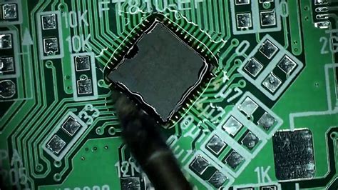
A QFN package is a surface-mount technology (SMT) package that has no leads extending from the package body. Instead, the electrical contacts are located on the bottom surface of the package in the form of exposed copper pads. The package is typically square or rectangular in shape and has a thin profile, making it suitable for space-constrained applications.
Advantages of QFN Packages
QFN packages offer several advantages over traditional leaded packages:
- Smaller footprint: QFN packages have a smaller footprint compared to leaded packages, allowing for higher component density on the PCB.
- Improved thermal performance: The exposed copper pad on the bottom of the package provides excellent thermal conductivity, enabling efficient heat dissipation from the chip to the PCB.
- Enhanced electrical performance: The short electrical paths in QFN packages reduce parasitic inductance and capacitance, resulting in improved signal integrity and faster switching speeds.
- Cost-effectiveness: QFN packages are less expensive to manufacture compared to leaded packages, making them an attractive option for cost-sensitive applications.
QFN Soldering Challenges
Despite their advantages, QFN packages present some challenges during the soldering process:
- Limited access to solder joints: The absence of leads makes it difficult to visually inspect the solder joints, as they are hidden underneath the package.
- Thermal dissipation: The small size of QFN packages and the limited thermal mass of the exposed copper pad can lead to rapid heating and cooling during soldering, which can cause thermal stress and potentially result in solder joint failures.
- Moisture sensitivity: QFN packages are prone to moisture absorption, which can cause package cracking or delamination during the soldering process if not handled properly.
- Voiding: The presence of voids in the solder joints can compromise the mechanical and electrical integrity of the connection, leading to reliability issues.

Board Layout Considerations for QFN Soldering
To mitigate the challenges associated with QFN soldering and ensure reliable solder joints, consider the following board layout guidelines:
1. Pad Design
The pad design for QFN packages is critical for achieving good solderability and reliable connections. Follow these recommendations:
- Use non-solder mask defined (NSMD) pads: NSMD pads have the solder mask opening larger than the copper pad, allowing for better solder wetting and improved alignment during placement.
- Provide adequate pad size: Ensure that the pad size is large enough to accommodate the package dimensions and any variations in the manufacturing process. A typical pad size for QFN packages is 1.0 to 1.2 times the nominal lead width.
- Include a Thermal Pad: The exposed copper pad on the bottom of the QFN package, known as the thermal pad or exposed pad, should be connected to a corresponding thermal pad on the PCB. The thermal pad helps dissipate heat from the package and provides mechanical stability. Size the thermal pad appropriately based on the package dimensions and the thermal requirements of the application.
2. Solder Mask Design
Proper solder mask design is essential for preventing solder bridging and ensuring adequate solder coverage. Consider these guidelines:
- Provide solder mask clearance: Maintain a sufficient solder mask clearance around the pads to prevent solder mask from encroaching onto the copper area. A typical solder mask clearance is 50 to 75 microns.
- Use solder mask between pads: Apply solder mask between adjacent pads to prevent solder bridging during the soldering process. The solder mask width between pads should be at least 0.15 mm.
- Define solder mask opening for the thermal pad: Create a solder mask opening for the thermal pad that is slightly smaller than the copper area. This helps contain the solder on the thermal pad and prevents it from spreading to adjacent pads.
3. Stencil Design
The stencil design plays a crucial role in ensuring the right amount of solder paste is deposited on the pads. Follow these recommendations:
- Use a stencil thickness of 0.125 to 0.150 mm: A stencil thickness in this range provides a good balance between solder volume and printability.
- Aperture size and shape: The aperture size should be slightly smaller than the pad size to prevent solder bridging. A typical aperture reduction is 10 to 20 percent. Use rectangular apertures for the perimeter pads and a square or circular aperture for the thermal pad.
- Consider stencil type: Laser-Cut Stencils offer better accuracy and consistency compared to chemically etched stencils. Electropolished stencils can further improve paste release and print quality.
4. Via Placement
Vias play an important role in providing electrical and thermal connections between layers on the PCB. Consider these guidelines for via placement:
- Thermal vias: Place thermal vias within the thermal pad area to enhance heat transfer from the package to the inner layers and the opposite side of the PCB. The number and size of thermal vias depend on the thermal requirements of the application.
- Via-in-pad: In some cases, it may be necessary to place vias within the pads to route signals to inner layers. Use filled or capped vias to prevent solder wicking and ensure a smooth surface for component placement.
- Via spacing: Maintain sufficient spacing between vias to prevent solder bridging and to allow for adequate solder coverage on the pads.
5. Placement and Routing
Proper placement and routing techniques can help minimize the impact of thermal stress and improve the overall reliability of the solder joints. Consider these guidelines:
- Orientation: Orient the QFN package such that the longer side is parallel to the direction of the board’s maximum thermal expansion. This helps reduce the shear stress on the solder joints caused by CTE mismatch.
- Symmetrical placement: Place components symmetrically around the QFN package to balance the thermal and mechanical stresses during soldering.
- Routing: Route traces away from the QFN package at a 45-degree angle to minimize stress concentration points. Avoid routing traces between the pads of the QFN package to prevent solder bridging.

Thermal Considerations
Thermal management is critical for QFN packages to ensure reliable operation and prevent overheating. Consider these thermal management techniques:
- Copper pours: Use copper pours on the top and bottom layers of the PCB to improve heat spreading and dissipation. Connect the copper pours to the thermal pad and vias to create a low-resistance thermal path.
- Thermal vias: As mentioned earlier, place thermal vias within the thermal pad area to transfer heat to the inner layers and the opposite side of the PCB. The number and size of thermal vias depend on the thermal requirements of the application.
- Heatsinks: In high-power applications, consider using heatsinks to dissipate heat from the QFN package. The heatsink can be attached to the top of the package or to the exposed copper area on the opposite side of the PCB.
- Airflow: Ensure adequate airflow around the QFN package to facilitate convective cooling. Use thermal simulation tools to analyze the airflow patterns and optimize the placement of components and vents.

Soldering Process Considerations
In addition to board layout, the soldering process itself plays a crucial role in achieving reliable QFN solder joints. Consider these process-related factors:
- Solder paste selection: Use a solder paste with the appropriate particle size and flux activity for QFN packages. Type 3 or Type 4 solder paste is commonly used for QFN soldering.
- Reflow profile: Develop a reflow profile that meets the specifications of the QFN package and the solder paste. The profile should have a controlled ramp rate, a well-defined peak temperature, and sufficient time above the liquidus temperature to ensure complete solder melting and wetting.
- Moisture sensitivity: QFN packages are moisture-sensitive devices (MSDs) and require proper handling and storage to prevent moisture absorption. Follow the manufacturer’s recommendations for moisture sensitivity level (MSL) classification and baking requirements.
- Inspection: Due to the limited access to solder joints, use X-ray inspection to verify the quality of QFN solder joints. X-ray inspection can reveal voids, bridging, and other defects that are not visible through optical inspection.
Frequently Asked Questions (FAQ)
- What is the recommended pad size for QFN packages?
-
The recommended pad size for QFN packages is typically 1.0 to 1.2 times the nominal lead width. This ensures adequate solder coverage and helps accommodate any variations in the manufacturing process.
-
How do thermal vias help in QFN soldering?
-
Thermal vias help transfer heat from the QFN package to the inner layers and the opposite side of the PCB. They provide a low-resistance thermal path, allowing for efficient heat dissipation and preventing overheating of the package.
-
What is the purpose of the solder mask between pads in QFN soldering?
-
The solder mask between pads acts as a barrier to prevent solder bridging during the soldering process. It helps contain the solder within the designated pad areas and maintains electrical isolation between adjacent pads.
-
Why is X-ray inspection important for QFN solder joints?
-
X-ray inspection is important for QFN solder joints because it allows for the detection of defects that are not visible through optical inspection. QFN packages have limited access to solder joints, making it difficult to visually inspect the quality of the connections. X-ray inspection can reveal voids, bridging, and other internal defects.
-
What is the recommended stencil thickness for QFN soldering?
- The recommended stencil thickness for QFN soldering is typically 0.125 to 0.150 mm. This thickness provides a good balance between solder volume and printability, ensuring adequate solder paste deposition on the pads.
Conclusion
Reliable soldering of QFN packages requires careful consideration of board layout, thermal management, and process control. By following the guidelines discussed in this article, designers can optimize their board layout for QFN soldering, minimizing the risk of defects and ensuring robust solder joints. Key aspects to consider include pad design, solder mask design, stencil design, via placement, and thermal management techniques. Additionally, selecting the appropriate solder paste, developing a suitable reflow profile, and conducting thorough inspections are essential for achieving reliable QFN solder joints. By addressing these factors, designers can take full advantage of the benefits offered by QFN packages while ensuring the long-term reliability of their electronic assemblies.


Leave a Reply