Introduction to BGA-PCB
Ball Grid Array (BGA) is a surface-mount packaging technology that has revolutionized the world of printed circuit board (PCB) assembly. BGA Packages offer numerous advantages over traditional through-hole and surface-mount technologies, making them a popular choice for high-density, high-performance electronic devices. In this comprehensive article, we will explore the various aspects of BGA in PCB Assembly, including its types, benefits, and inspection techniques.
What is BGA?
BGA is a type of surface-mount technology (SMT) package that uses an array of solder balls to connect the integrated circuit (IC) to the PCB. The solder balls are arranged in a grid pattern on the bottom side of the package, allowing for a high number of interconnections in a small area. BGA packages can have hundreds or even thousands of solder balls, depending on the size and complexity of the IC.
Advantages of BGA over traditional packaging
Compared to traditional through-hole and surface-mount packages, BGA offers several advantages:
- Higher pin density: BGA packages can accommodate a large number of interconnections in a small footprint, making them ideal for high-density PCB designs.
- Better electrical performance: The short lead lengths and low inductance of BGA packages result in improved signal integrity and reduced noise.
- Enhanced thermal performance: The large surface area of the solder ball array allows for better heat dissipation, which is crucial for high-power devices.
- Increased reliability: BGA packages have a lower profile and are less susceptible to mechanical stress, resulting in improved reliability.

Types of BGA Packages
There are several types of BGA packages, each designed to meet specific requirements and applications. Some of the most common types include:
Plastic BGA (PBGA)
PBGA is the most widely used type of BGA package. It consists of a plastIC Substrate with a die attached to the top side and an array of solder balls on the bottom side. PBGA packages are cost-effective and suitable for a wide range of applications.
Ceramic BGA (CBGA)
CBGA packages use a ceramic substrate instead of plastic, offering better thermal and electrical performance. They are more expensive than PBGA packages and are typically used in high-reliability applications, such as aerospace and defense.
Tape BGA (TBGA)
TBGA packages use a flexible tape substrate, which allows for thinner and lighter packages. They are commonly used in mobile devices and other space-constrained applications.
Flip Chip BGA (FCBGA)
FCBGA packages use a flip-chip die attachment method, where the die is directly connected to the substrate using solder bumps. This eliminates the need for wire bonding, resulting in improved electrical performance and reduced package size.
| BGA Type | Substrate Material | Key Features | Typical Applications |
|---|---|---|---|
| PBGA | Plastic | Cost-effective, widely used | Consumer electronics, telecommunications |
| CBGA | Ceramic | High thermal and electrical performance, expensive | Aerospace, defense, high-reliability applications |
| TBGA | Flexible tape | Thin and lightweight | Mobile devices, space-constrained applications |
| FCBGA | Varies | Flip-chip die attachment, improved electrical performance, reduced size | High-performance computing, networking |

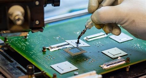
BGA-PCB Assembly Process
The BGA-PCB assembly process involves several steps, each requiring precise control and attention to detail. The main steps in the process are:
- Solder paste printing: A stencil is used to apply solder paste to the PCB pads where the BGA package will be placed.
- Component placement: The BGA package is accurately positioned on the PCB using a pick-and-place machine.
- Reflow soldering: The PCB is heated in a reflow oven, causing the solder paste to melt and form a reliable connection between the BGA package and the PCB.
- Inspection: The assembLED PCB undergoes various inspection techniques to ensure the quality and reliability of the solder joints.
Challenges in BGA-PCB Assembly
BGA-PCB assembly presents several challenges due to the high density and small size of the solder balls. Some of the key challenges include:
- Accurate placement: Precise alignment of the BGA package with the PCB pads is critical to ensure proper solder joint formation.
- Warpage control: Both the BGA package and the PCB can experience warpage during the reflow process, leading to poor solder joint quality.
- Void formation: Voids can form within the solder joints, reducing their strength and reliability.
- Thermal management: High-power BGA devices generate significant heat, which must be effectively dissipated to prevent thermal damage to the package and PCB.

BGA Inspection Techniques
Ensuring the quality and reliability of BGA solder joints is crucial for the overall performance and longevity of the electronic device. Several inspection techniques are used to assess the integrity of BGA solder joints, including:
X-ray Inspection
X-ray inspection is a non-destructive technique that allows for the visualization of solder joints beneath the BGA package. It can detect defects such as voids, bridging, and insufficient solder.
Automated Optical Inspection (AOI)
AOI uses high-resolution cameras and image processing algorithms to inspect the surface of the PCB for defects such as misaligned components, solder bridging, and insufficient solder.
Boundary Scan Testing
Boundary scan testing, also known as JTAG testing, is a functional test method that uses a built-in test access port (TAP) to assess the interconnections between ICs on a PCB. It can detect defects such as open and short circuits.
Acoustic Micro Imaging (AMI)
AMI uses high-frequency ultrasound to create a 3D image of the solder joints, allowing for the detection of voids, delamination, and other internal defects.
| Inspection Technique | Defects Detected | Advantages | Limitations |
|---|---|---|---|
| X-ray Inspection | Voids, bridging, insufficient solder | Non-destructive, can visualize hidden joints | Limited resolution, cannot detect surface defects |
| AOI | Misaligned components, solder bridging, insufficient solder | Fast, automated, can detect surface defects | Cannot detect internal defects |
| Boundary Scan Testing | Open and short circuits | Functional test, can detect interconnection defects | Requires built-in TAP, cannot detect physical defects |
| AMI | Voids, delamination, internal defects | Can visualize internal structure of joints | Slow, requires specialized equipment |
Benefits of BGA in PCB Assembly
The use of BGA packages in PCB assembly offers numerous benefits, making them an attractive choice for a wide range of applications. Some of the key benefits include:
- Miniaturization: BGA packages enable the design of smaller, more compact electronic devices, which is essential for mobile and wearable applications.
- Improved performance: The short lead lengths and low inductance of BGA packages result in better signal integrity and faster signal propagation, enabling higher-speed devices.
- Increased functionality: The high pin density of BGA packages allows for the integration of more features and functions into a single device.
- Enhanced reliability: BGA packages have a lower profile and are less susceptible to mechanical stress, resulting in improved reliability and longer product life.
- Cost-effective: Despite the initial investment in BGA assembly equipment, the overall cost of BGA-PCB assembly can be lower due to reduced board size and increased production efficiency.
Future Trends in BGA-PCB Assembly
As electronic devices continue to evolve and become more complex, BGA-PCB assembly technologies must adapt to meet new challenges and demands. Some of the future trends in BGA-PCB assembly include:
- Smaller pitch: The pitch, or distance between solder balls, is expected to decrease further, enabling even higher pin densities and more compact packages.
- Advanced materials: New substrate materials, such as high-density interconnect (HDI) and embedded die substrates, will enable the development of more complex and high-performance BGA packages.
- 3D packaging: The use of 3D packaging technologies, such as package-on-package (PoP) and through-silicon via (TSV), will allow for the vertical stacking of multiple BGA packages, further increasing device density and functionality.
- Improved inspection methods: Advances in inspection technologies, such as 3D X-ray and laser ultrasound, will enable more accurate and efficient detection of defects in BGA solder joints.
Frequently Asked Questions (FAQ)
- What is the difference between BGA and QFN packages?
-
BGA packages have an array of solder balls on the bottom side, while QFN (Quad Flat No-lead) packages have a flat bottom surface with exposed pads along the edges. BGA packages offer higher pin density and better thermal performance, while QFN packages are smaller and less expensive.
-
Can BGA packages be reworked?
-
Yes, BGA packages can be reworked, but it requires specialized equipment and expertise. The rework process involves removing the defective package, cleaning the PCB pads, and soldering a new package in its place.
-
How does the size of solder balls affect BGA performance?
-
Smaller solder balls allow for higher pin density and more compact packages, but they also present challenges in terms of solder joint reliability and inspection. Larger solder balls offer better mechanical strength and are easier to inspect but limit the package density.
-
What is the role of underfill in BGA-PCB assembly?
-
Underfill is an epoxy material that is applied between the BGA package and the PCB after soldering. It helps to distribute mechanical stress, improve thermal performance, and enhance the reliability of the solder joints.
-
How can warpage be minimized in BGA-PCB assembly?
- Warpage can be minimized by using materials with matched coefficients of thermal expansion (CTE), optimizing the reflow profile, and employing techniques such as corner bonding and edge bonding. Proper PCB design and packaging selection can also help to reduce warpage.
Conclusion
BGA packages have become an essential component in modern PCB assembly, offering numerous advantages in terms of density, performance, and reliability. As electronic devices continue to advance, BGA technologies will evolve to meet new challenges and enable the development of even more innovative and compact products. By understanding the types, benefits, and inspection techniques associated with BGA-PCB assembly, engineers and manufacturers can effectively harness the potential of this powerful packaging technology.


Leave a Reply