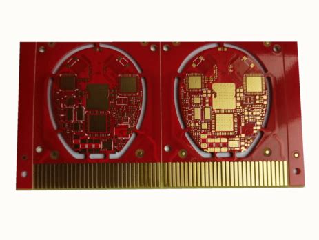
Introduction to Goldfinger PCB
Goldfinger PCB, also known as gold-plated printed circuit boards, are a type of high-quality PCB that features a layer of gold plating on the surface of the copper traces and pads. This gold plating provides several benefits, including enhanced corrosion resistance, improved solderability, and superior electrical conductivity. These characteristics make Goldfinger PCBs ideal for applications that demand high reliability, such as aerospace, military, and medical devices.
However, despite the numerous advantages of Goldfinger PCBs, they are not immune to quality issues. In this article, we will explore some of the common quality problems associated with gold-plated PCBs and discuss the measures that can be taken to mitigate these issues.
Common Quality Issues in Goldfinger PCBs
1. Gold Plating Thickness Variations
One of the most critical aspects of Goldfinger PCBs is the thickness of the gold plating layer. The ideal gold plating thickness ranges from 0.05 to 0.1 microns (2 to 4 microinches). If the gold plating is too thin, it may not provide adequate protection against corrosion or wear. On the other hand, if the plating is too thick, it can lead to issues such as poor solderability and increased cost.
Thickness variations can occur due to several factors, including:
- Inconsistent plating current density
- Uneven distribution of the plating solution
- Improper surface preparation before plating
To ensure consistent gold plating thickness, manufacturers must implement strict process controls and regularly monitor the plating process using techniques such as X-ray fluorescence (XRF) or cross-sectional analysis.
2. Pinholes and Porosity
Pinholes and porosity are small defects that can occur in the gold plating layer, exposing the underlying copper to the environment. These defects can lead to corrosion, reduced electrical conductivity, and decreased reliability of the PCB.
Pinholes and porosity can be caused by:
- Contamination of the plating solution
- Inadequate surface cleaning before plating
- Incorrect plating parameters (e.g., current density, temperature)
To minimize the occurrence of pinholes and porosity, manufacturers must maintain a clean plating environment, use high-quality Plating Solutions, and optimize the plating process parameters.
3. Adhesion Issues
Proper adhesion between the gold plating layer and the underlying copper is essential for the long-term reliability of Goldfinger PCBs. Poor adhesion can lead to delamination, blistering, or peeling of the gold layer, exposing the copper to the environment and compromising the PCB’s performance.
Adhesion issues can be caused by:
- Inadequate surface preparation (e.g., insufficient cleaning or roughening)
- Contamination of the copper surface before plating
- Incorrect plating process parameters (e.g., low current density)
To ensure good adhesion, manufacturers must follow strict surface preparation protocols, maintain a clean plating environment, and optimize the plating process parameters.
4. Nodules and Dendrites
Nodules and dendrites are small, irregular growths that can form on the surface of the gold plating layer. These growths can cause short circuits, reduce the PCB’s insulation resistance, and compromise its overall reliability.
Nodules and dendrites can be caused by:
- Excessive plating current density
- Contamination of the plating solution
- Inadequate filtration of the plating solution
To prevent the formation of nodules and dendrites, manufacturers must maintain the plating solution’s purity, use appropriate filtration systems, and control the plating current density within the recommended range.

Measures to Ensure Goldfinger PCB Quality
To address the quality issues associated with Goldfinger PCBs, manufacturers can implement several measures:
1. Strict Process Control
Maintaining strict control over the entire PCB manufacturing process is crucial for ensuring the quality of Goldfinger PCBs. This includes:
- Implementing a robust quality management system (QMS)
- Establishing and adhering to standard operating procedures (SOPs)
- Regularly calibrating and maintaining equipment
- Conducting in-process inspections and testing
2. Material Selection and Qualification
Using high-quality materials is essential for producing reliable Goldfinger PCBs. Manufacturers should:
- Select reputable suppliers for PCB substrates, copper foils, and plating solutions
- Qualify materials through rigorous testing and evaluation
- Regularly audit suppliers to ensure consistent material quality
3. Advanced Inspection Techniques
Employing advanced inspection techniques can help detect and prevent quality issues in Goldfinger PCBs. Some of these techniques include:
- Automated optical inspection (AOI) for detecting surface defects
- X-ray inspection for identifying internal defects and measuring plating thickness
- Ionic contamination testing for assessing the cleanliness of the PCB surface
4. Employee Training and Skill Development
Investing in employee training and skill development is essential for maintaining a high level of quality in Goldfinger PCB production. Manufacturers should:
- Provide regular training on best practices and quality control procedures
- Encourage employees to pursue relevant certifications (e.g., IPC Standards)
- Foster a culture of continuous improvement and problem-solving

Frequently Asked Questions (FAQ)
-
Q: What is the difference between Goldfinger PCBs and standard PCBs?
A: Goldfinger PCBs feature a layer of gold plating on the surface of the copper traces and pads, providing enhanced corrosion resistance, improved solderability, and superior electrical conductivity compared to standard PCBs. -
Q: What are the main applications for Goldfinger PCBs?
A: Goldfinger PCBs are commonly used in applications that require high reliability, such as aerospace, military, and medical devices. They are also used in high-frequency and RF applications due to their excellent electrical properties. -
Q: How can I ensure the quality of Goldfinger PCBs in my products?
A: To ensure the quality of Goldfinger PCBs, work with reputable manufacturers who implement strict process controls, use high-quality materials, and employ advanced inspection techniques. Additionally, consider conducting your own incoming quality control (IQC) inspections and testing. -
Q: What is the recommended gold plating thickness for Goldfinger PCBs?
A: The ideal gold plating thickness for Goldfinger PCBs ranges from 0.05 to 0.1 microns (2 to 4 microinches). This thickness range provides an optimal balance between corrosion protection, solderability, and cost-effectiveness. -
Q: How can I prevent corrosion on Goldfinger PCBs?
A: To prevent corrosion on Goldfinger PCBs, ensure that the gold plating thickness is within the recommended range and free from defects such as pinholes and porosity. Additionally, store and handle PCBs in a clean, dry environment and use appropriate packaging materials to minimize exposure to corrosive agents.

Conclusion
Goldfinger PCBs offer numerous benefits, including enhanced corrosion resistance, improved solderability, and superior electrical conductivity. However, they are not immune to quality issues such as gold plating thickness variations, pinholes and porosity, adhesion issues, and nodules and dendrites.
To mitigate these quality issues, manufacturers must implement strict process controls, use high-quality materials, employ advanced inspection techniques, and invest in employee training and skill development. By adhering to best practices and continuously improving their processes, manufacturers can produce high-quality Goldfinger PCBs that meet the demanding requirements of various applications.
As a consumer or designer, it is essential to work with reputable Goldfinger PCB Manufacturers who prioritize quality and reliability. By doing so, you can ensure that your products benefit from the superior performance and durability offered by gold-plated PCBs, ultimately leading to increased customer satisfaction and success in the marketplace.


Leave a Reply