The Importance of PCB Inspections
PCB inspections are essential for identifying defects, ensuring compliance with design specifications, and maintaining the overall quality of the assembLED PCBs. By conducting rigorous inspections at various stages of the assembly process, manufacturers can detect and rectify issues early on, preventing costly rework and delays. Moreover, PCB inspections help to:
- Reduce the risk of product failures and warranty claims
- Enhance the reliability and performance of the final product
- Improve customer satisfaction and brand reputation
- Comply with industry standards and regulations
Types of PCB Inspections
There are several types of PCB inspections that are conducted during the one-stop PCB Assembly process. These inspections can be broadly categorized into visual inspections, automated optical inspections (AOI), and electrical tests.
1. Visual Inspections
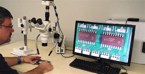
Visual inspections are the most basic form of PCB inspection and are typically performed by trained operators using magnifying lenses or microscopes. These inspections focus on identifying surface-level defects such as:
- Solder bridges or shorts
- Insufficient or excessive solder
- Component placement and orientation
- Contamination or foreign objects
- Damaged or missing components
While visual inspections are relatively simple and cost-effective, they are prone to human error and may not detect more subtle defects.
2. Automated Optical Inspections (AOI)
Automated optical inspections (AOI) use high-resolution cameras and advanced software algorithms to scan the PCB surface and compare it to the original design data. AOI systems can detect a wide range of defects, including:
- Incorrect component placement or orientation
- Solder joint defects (e.g., insufficient, excessive, or missing solder)
- Pad and trace defects
- Damaged or missing components
- Solder mask and silkscreen defects
AOI is a fast and reliable method of inspection that can significantly reduce the time and cost associated with manual inspections. However, AOI systems may have limitations in detecting certain types of defects, such as those hidden under components or within the PCB Layers.
3. Electrical Tests
Electrical tests are performed to verify the functionality and performance of the assembled PCBs. These tests can be further divided into in-circuit testing (ICT) and functional testing.
In-Circuit Testing (ICT)
In-circuit testing involves using specialized equipment to test the individual components and interconnections on the PCB. ICT systems typically use a bed-of-nails fixture to make contact with the PCB’s test points and measure the electrical characteristics of each component. ICT can detect defects such as:
- Short circuits or open connections
- Incorrect component values or tolerances
- Missing or damaged components
- Reversed polarity components
ICT is a highly effective method of detecting manufacturing defects and ensuring the correct assembly of the PCB. However, it requires the design and fabrication of custom test fixtures, which can be costly and time-consuming.
Functional Testing
Functional testing involves powering up the assembled PCB and verifying its performance under real-world operating conditions. This type of testing can be performed using automated test equipment (ATE) or by manually testing the PCB’s inputs and outputs. Functional testing can detect issues such as:
- Incorrect signal integrity or timing
- Electromagnetic interference (EMI) or compatibility issues
- Software or firmware bugs
- Thermal or power management problems
Functional testing is essential for ensuring that the assembled PCB meets the intended design specifications and performs reliably in the end-use application.
Best Practices for PCB Inspections in One-Stop PCB Assembly
To ensure the effectiveness and efficiency of PCB inspections in one-stop PCB assembly, manufacturers should follow these best practices:
-
Implement a comprehensive quality management system (QMS) that includes well-defined inspection procedures, acceptance criteria, and documentation requirements.
-
Invest in state-of-the-art inspection equipment, such as high-resolution AOI systems and advanced electrical test solutions, to maximize defect detection capabilities.
-
Provide regular training and certification for inspection personnel to ensure they have the necessary skills and knowledge to perform their tasks effectively.
-
Collaborate closely with customers to understand their specific quality requirements and develop customized inspection plans that meet their needs.
-
Continuously monitor and analyze inspection data to identify trends, root causes of defects, and opportunities for process improvement.
-
Implement a robust corrective and preventive action (CAPA) system to address identified defects and prevent their recurrence in future production runs.
-
Regularly audit and validate the inspection processes to ensure their ongoing effectiveness and compliance with industry standards and regulations.

The Benefits of One-Stop PCB Assembly with Comprehensive Inspections
By partnering with a one-stop PCB assembly provider that offers comprehensive inspection services, customers can enjoy numerous benefits, such as:
-
Reduced time-to-market: With all aspects of PCB assembly, including inspections, handled under one roof, customers can expect faster turnaround times and shorter product development cycles.
-
Enhanced quality and reliability: Rigorous inspections at every stage of the assembly process help to identify and eliminate defects early on, resulting in higher-quality PCBs with improved reliability and performance.
-
Cost savings: By detecting and correcting defects early in the assembly process, one-stop PCB assembly providers can help customers avoid costly rework, scrap, and warranty claims.
-
Streamlined communication and collaboration: Working with a single point of contact for all PCB assembly needs, including inspections, enables better communication, faster issue resolution, and a more seamless overall experience for customers.
-
Access to expertise and advanced technologies: One-stop PCB assembly providers typically invest in the latest inspection equipment and employ experienced professionals, giving customers access to cutting-edge technologies and expertise that may not be available in-house.

Conclusion
PCB inspections are a critical component of one-stop PCB assembly, ensuring the quality, reliability, and performance of the final product. By incorporating visual inspections, automated optical inspections (AOI), and electrical tests into the assembly process, manufacturers can detect and rectify defects early on, reducing costs and improving customer satisfaction. Partnering with a one-stop PCB assembly provider that offers comprehensive inspection services can help customers streamline their product development efforts, enhance product quality, and gain a competitive edge in the market.

FAQs
-
What are the most common types of defects detected during PCB inspections?
Some of the most common defects detected during PCB inspections include solder joint defects (e.g., bridges, insufficient or excessive solder), component placement and orientation issues, damaged or missing components, and trace or pad defects. -
How do I choose the right one-stop PCB assembly provider for my inspection needs?
When choosing a one-stop PCB assembly provider, consider factors such as their experience, expertise, inspection capabilities, quality management systems, and customer support. Look for providers that offer a wide range of inspection services, invest in advanced technologies, and have a proven track record of delivering high-quality PCBs. -
Can PCB inspections guarantee 100% defect-free products?
While PCB inspections are highly effective in detecting and reducing defects, no inspection method can guarantee 100% defect-free products. However, by implementing a comprehensive inspection strategy and following best practices, manufacturers can significantly minimize the risk of defects and improve the overall quality of the assembled PCBs. -
How can I ensure that my PCB Design is optimized for manufacturability and inspectability?
To optimize your PCB design for manufacturability and inspectability, follow industry-standard design guidelines, such as those provided by IPC (Association Connecting Electronics Industries). Collaborate closely with your one-stop PCB assembly provider to understand their specific manufacturing and inspection capabilities and incorporate their feedback into your design process. -
What are the latest trends and technologies in PCB inspections?
Some of the latest trends and technologies in PCB inspections include the use of 3D AOI systems for enhanced defect detection, the integration of artificial intelligence (AI) and machine learning algorithms for improved inspection accuracy and speed, and the adoption of Industry 4.0 technologies, such as the Internet of Things (IoT) and big data analytics, for real-time monitoring and process optimization.
| Inspection Type | Defects Detected | Advantages | Limitations |
|---|---|---|---|
| Visual Inspection | – Solder bridges or shorts – Insufficient or excessive solder – Component placement and orientation – Contamination or foreign objects – Damaged or missing components |
– Simple and cost-effective – Can detect surface-level defects |
– Prone to human error – May not detect subtle defects |
| Automated Optical Inspection (AOI) | – Incorrect component placement or orientation – Solder joint defects – Pad and trace defects – Damaged or missing components – Solder mask and silkscreen defects |
– Fast and reliable – Reduces time and cost compared to manual inspections – Can detect a wide range of defects |
– May have limitations in detecting defects hidden under components or within PCB layers |
| In-Circuit Testing (ICT) | – Short circuits or open connections – Incorrect component values or tolerances – Missing or damaged components – Reversed polarity components |
– Highly effective in detecting manufacturing defects – Ensures correct assembly of the PCB |
– Requires custom test fixtures, which can be costly and time-consuming |
| Functional Testing | – Incorrect signal integrity or timing – Electromagnetic interference (EMI) or compatibility issues – Software or firmware bugs – Thermal or power management problems |
– Verifies performance under real-world operating conditions – Ensures the PCB meets design specifications |
– May not detect all manufacturing defects – Can be time-consuming and resource-intensive |


Leave a Reply