Introduction to PCB milling
PCB milling, also known as mechanical milling or routing, is a process used to fabricate printed circuit boards (PCBs). It involves using a computer-controlled milling machine or router to physically remove copper from a substrate to create the traces, pads, and outlines of a PCB design.
PCB milling has traditionally been used for quick-turn prototyping of PCBs, but advances in milling machines and cutter technology have made it suitable for small-batch PCB production as well. It allows designers to quickly go from a completed design to a physical PCB without the costs and lead times associated with traditional PCB fabrication methods.
How PCB Milling Works
The PCB milling process starts with a custom PCB design created using CAD (computer-aided design) software. The PCB layout file is then imported into CAM (computer-aided manufacturing) software that is used to generate toolpaths for the milling machine.
Toolpaths provide the milling machine with the X, Y, and Z axis coordinates and instructions on where to move the cutter in order to mill away the unwanted copper. The toolpaths control the back and forth movement of the milling machine as the spinning end mill cutter removes the copper to create the traces, pads, vias, and board outline.
Precise control over the cutter path, depth, feed rates, and spindle speeds allows intricate PCB details to be milled away, leaving behind the desired conductor pattern on the substrate. The CAM software converts the PCB design into G-code or another numeric control programming language that can be read by the milling machine.
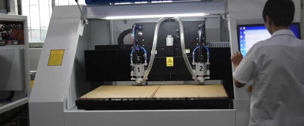
Equipment Used in PCB Milling
The primary pieces of equipment used in PCB milling include:
- CNC milling machine/PCB router – A computer numerically controlled (CNC) vertical milling machine or router designed specifically for PCB fabrication. It uses spinning end mill bits to mill away copper on the PCB substrate.
- End mills – The cutting tools used for removing copper during milling. Carbide end mills with 2-4 flutes are commonly used. Smaller diameter mills are used for finer details.
- Substrate – The insulating PCB substrate, usually FR-4 or some other fiberglass material for prototyping. The substrate has thin copper foil laminated to it.
- Fixturing – A method of holding and securing the PCB substrate during milling. This includes vacuum hold-down beds, clamps, vises, etc. Proper fixturing is critical for accurate milling.
- CAM software – Computer-aided manufacturing software is used for converting PCB designs into toolpaths and G-code for the milling machine. Common options include EagleCAM, PCB-GCODE, Visolate, and more.
- Coolant – Used to keep the end mill cool during milling, flush away milling debris, and prevent clogging. Water or water-soluble oil solutions are typical.
When to Use PCB Milling
Here are some of the main situations where PCB milling would be the preferred option over traditional PCB fabrication:
Prototyping
One of the biggest advantages of milling PCBs is the fast turn-around time, making it ideal for prototyping needs. Designs can be milled in hours or days versus weeks for traditional PCB fabrication. The ability to quickly iterate on a design is extremely beneficial during development and debugging.
Small Batch Production
For small production runs requiring less than ~50 boards, milling can be more cost effective than traditional fabrication. The equipment costs are much lower compared to the costs of photo tools and setup fees at factories. Milling is suitable for small startups or companies making custom PCBs in low volumes.
Low Volume Production
Even for production volumes of up to a few hundred boards per year, milling may be preferred. The shorter lead times allow companies to quickly produce boards on demand and avoid having to stockpile large inventories. Rush delivery is possible with milling.
Advanced Prototyping
Milling supports advanced PCB technologies like flexible substrates, HDI (high density interconnect), and more, allowing these techniques to be prototyped. Special fixtures and cutters are available to mill rigid-flex PCBs and other advanced boards not supported by basic prototyping services.
Design Changes
Engineers can quickly iterate on a design by making modifications and milling a new version of the board. Traditional fabrication requires designers to wait days or weeks if any changes are needed. Milling offers faster design modification turnaround times.
Education
Schools use PCB milling machines for education, allowing students to get hands-on PCB fabrication experience in the classroom. This provides valuable skills in taking a design to an actual finished board. Milling services are also popular for student projects and competitions.
Rare Materials
Milling allows the use of specialized or rare substrate materials that would be infeasible, extremely expensive, or impossible to source using traditional fabrication means. This includes things like aluminum PCBs. The material just needs to be available in sheet stock form.
PCB Milling Process Step-by-Step
Here is an overview of the complete workflow for milling a PCB from design to finished board:
1. Design
- Create the circuit schematic and PCB layout using EDA software like Eagle, KiCad, Altium, OrCAD, etc.
- The software will generate Gerber files needed for fabrication. NC drill files are also generated.
- Perform design rule checks to ensure manufacturability. Account for milling capabilities.
2. Generate Toolpaths
- Import Gerber and drill files into CAM software like EagleCAM, PCB-GCODE, FlatCAM, etc.
- Software processes files and generates toolpaths for all milling operations.
- Toolpaths converted to G-code instructions for the milling machine.
3. Prepare Equipment
- Install desired end mill in collet of milling machine. Select size based on features.
- Prepare substrate material and properly fixture in place. Vacuum beds commonly used.
- Set spindle RPM based on cutter diameter and material. Copper foil usually ~25,000 RPM.
- Coolant delivery setup to milling area. Water or water-soluble oil often used.
4. Surface Milling
- First operation mills away entire copper surface to isolate all traces.
- Multiple toolpath passes used to clear large areas. 0.01″ to 0.02″ depth per pass.
- Larger end mills (1/64″ to 1/32″) used first then smaller mills for finer details.
5. Trace Milling
- Toolpaths mill out areas between traces to electrically isolate conductors.
- Small end mills (0.01″ to 0.005″) allow intricate details and spacing.
- Multipass approach used with small stepdowns ~0.002″ to 0.005″ per pass.
6. Hole Drilling
- Holes are drilled using NC drill coordinate file.
- Standard PCB drill bits used, usually starting with larger sizes then smaller.
- Holes may be finished to final size by milling with smaller end mills.
7. Edge Milling
- Final toolpaths cut out board outline from substrate.
- 0.001″ to 0.005″ stepdowns used around perimeter.
- PCB edges can also be routed or broken manually.
8. Finish
- Remove any burrs with small end mill. clean board with brush.
- Optional steps like solder mask application or routing edges can be done.
- PCB is now ready for final inspection, testing, and assembly.
Advantages and Disadvantages of PCB Milling
Advantages
- Fast turnaround times – Hours or days vs weeks for fabrication
- Lower costs for prototypes and small batches
- Suitable for quick design iterations and changes
- Allows use of specialized materials like flex PCBs
- Provides educational opportunities for students
Disadvantages
- Limited fine feature size and spacing vs etching
- More hands-on labor involved in process
- Requires knowledge of G-code and CAM software
- Lower dimensional accuracy compared to fabrication
- Limited to smaller board sizes, usually under 8″x8″
- Surface finish and tolerances not as precise
- Requires equipment maintenance and skilled operators
Key Milling Machine Specifications
PCB milling machines come in a variety of sizes, capabilities and prices. Here are some of the key factors to consider when selecting a PCB milling machine:
- Work Area – Maximum x/y dimensions of PCB it can accommodate. Typical sizes range from ~4″x4″ to 12″x12″.
- Spindle Speed – Maximum spindle/bit RPM. Higher speeds (~25,000+ RPM) preferred for milling copper.
- Cutting Depth – Maximum depth it can mill in a single pass. 1mm to 2mm depth is suitable for PCBs.
- Minimum Geometry – The smallest line width or feature it can mill. Varies ~0.005″ to 0.010″ for hobbyist models.
- Positioning Accuracy – Precision of x/y motion system. Around 0.001″ accuracy typical for most machines.
- Repeatability – Ability to return to the same position consistently. ~0.002″ or better repeatability ideal.
- Cost – Initial machine investment. Entry models ~$1000 to $4000. High-end machines can cost over $50,000.
- Supported Materials – PCB substrate materials it can mill like FR-4, aluminum, etc. Flexible PCB capability.
- Software – CAD/CAM software options compatible with the machine. Open-source vs proprietary.
Tooling for PCB Milling
Having the right cutting tools is critical in order to achieve good milling results. Here are the key types of end mills used:
Ball Nose End Mills
- Also called ball end mills. Rounded end allows 3D contour milling.
- Primarily used for isolation milling of entire copper surface.
- Come in a range of sizes. Larger mills used for roughing passes.
- 2 flute and 4 flute common. Higher flute count improves finish.
- Typical diameter range of 1/32″ to 1/8″ (0.8mm to 3.175mm).
Tapered End Mills
- Referred to as taper mills or v-bits. Angled conical shape.
- Allows access into tight spaces and sharp corners.
- Well suited for trace isolation milling requiring high precision.
- Diameters options range from 0.01″ to 0.04″ (0.25mm to 1mm).
Straight End Mills
- End cutting mills with straight cylindrical shank.
- Used for slotting, side milling, and edge profiling operations.
- Allows plunging straight down.
- Come in square and corner radius variations.
- Typical size range of 0.01″ to 0.1″ (0.25mm to 2.5mm) diameter.
Drill Bits
- For drilling hole locations through the PCB substrate.
- Standard twist drill bits normally used.
- Sizes match hole diameters called out in drill drawing file.
- Carbide material recommended foroptimal wear resistance and life.
- May also use end mills in smaller diameters for holes.
PCB Milling Feeds and Speeds
The cutting parameters on the milling machine greatly impact the milling results. Using properly calculated feeds and speeds is critical. Here are guidelines on settings to use when cutting copper clad PCB substrates:
Spindle Speed
- Standard cutting speed for milling copper is 600 to 1000 SFM (Surface feet per minute)
- With small cutter diameters, this requires spindle RPMs of 25,000 to 45,000.
- Formula: Spindle RPM = (12 x SFM) / (Pi x Cutter Dia. in inches)
- Always stay within max safe RPM given for specific end mill dimensions.
Feed Rate
- The speed the cutter is moved in the X/Y axes during milling.
- For copper, use feed rates from 30 to 80 IPM (inches per minute).
- Decrease feed rate for finer finish requirements.
- Can be programmed or adjusted on machine during milling.
Stepdown
- The depth per pass during trace isolation and profiling.
- Typical range of 0.001″ to 0.005″ stepdown per pass.
- Larger stepdowns possible with smaller end mills.
- Finer stepdowns required for tighter tolerances.
Plunge Rate
- The feed rate moving vertically down into material (Z-axis).
- Use 10% to 30% of normal feed rate.
- Very slow plunge rates needed for drilled holes. As low as 10 IPM.
- Helps prevent cutter breakage and damage.
PCB Miller Machine Maintenance
Maintaining a PCB milling machine helps maximize uptime, extend tool life, and produce quality boards. Here are key maintenance activities:
- Cleaning – Keep machine free of debris, dust, and grime which can affect precision. Clean ways and lubricate X/Y rails/screws regularly.
- Inspections – Check for any loose mechanical parts. Ensure travel is smooth without binding. Inspect electrical cabling condition.
- Coolant System – Change or filter coolant regularly to avoid clogs and clean debris from pump intake strainers often.
- Leveling – Verify machine base remains properly leveled. Improper leveling affects accuracy. Check after moving machine or periodically.
- Cutters – Inspect end mills regularly for any signs of wear, chips, or breakage then replace as needed. Proper handling/storage of cutters is critical.
- Spindle – Lubricate spindle shaft and use balanced cutters. Periodically check runout. Replace bearings if any play develops.
- Filters – Clean/change dust collection system filters as required. Ensure good chip evacuation.
- Accuracy – Verify calibration periodically by test milling known geometric patterns and making measurements. Re-calibrate as required.
PCB Milling Accuracy and Tolerances
Here is an overview of typical accuracy and fabrication tolerances associated with milled PCBs:
Dimensional Accuracy
- The precision of milled PCB feature sizes and locations.
- Depends largely on machine positioning accuracy specification.
- Around +/- 0.002″ (0.05mm) accuracy is common.
- Better than +/- 0.001″ (0.025mm) achievable with precision machines.
Line Width and Spacing
- The smallest trace width and spacing between traces is limited by end mill diameter.
- Hobby machines usually limited to > 0.005″ (0.127mm) trace/space.
- On more advanced mills > 0.003″ (0.076mm) traces are possible.
Registration
- How precisely different milling operations align.
- Affected by accuracy, repeatability, and fixture method.
- Typically around +/- 0.003″ to 0.005″ registration.
- Registration can be improved by adding fiducials.
Hole Location
- Positional accuracy of drilled holes.
- Similar factors affect hole placement precision.
- Often +/- 0.003″ to 0.005″ hole location tolerance.
- Hole diameter tolerances around +/- 0.001″ to 0.003″
Frequently Asked Questions
What materials can be used for PCB milling?
The most common material is FR-4 fiberglass, but others like Rogers high frequency boards, flexible circuit materials, and even metals like aluminum can be milled. The key requirement is that the material can be held flat in sheet form for milling.
What thickness of materials can be milled?
Standard 1.6mm (0.062″) FR-4 is common, but any thickness from 0.8mm to 6mm can typically be handled depending on the machine. Thinner flex circuit materials can be milled with proper fixturing techniques.
How many PCBs can be milled at once?
Usually only one board is milled at a time. Multiple boards can be batched by stacking substrates and using longer end mills to cut through the stack. This is limited to simpler designs.
How precise are milled PCBs compared to commercial fabrication?
Milled PCBs are less precise with tolerances around +/- 5 mils versus +/- 2 mils for fabrication. Line width/spacing is limited, usually > 5 mil traces are possible. Registration is also more of a challenge.
Can solder mask and silkscreening be done with milled PCBs?
Yes, solder mask and silkscreen layers can be applied after milling using liquid photoimageable solder mask and toner transfer for silkscreen. This enhances the overall quality and finish.
How long does it take to mill a typical PCB?
Simple boards may take under an hour. More complex boards with fine features can take many hours to do all the milling operations. Time depends largely on board size and detailed area.


Leave a Reply