A PCB (printed circuit board) mount refers to the method by which a component is mechanically fastened and electrically connected to a PCB. There are several common PCB mount styles, each with their own benefits and drawbacks depending on the application. Some key types of PCB mounts include:
Through-Hole Mount
Overview
Through-hole mounting involves component leads or terminals being inserted into holes drilled in the PCB and soldered on the opposite side to create both a mechanical and electrical connection.
Advantages
- Strong mechanical connection to PCB
- Simple manufacturing and component installation
- Well suited for high vibration environments
- Easy visual inspection of solder joints
Disadvantages
- Requires drilling holes in PCB which takes up space
- Unable to mount components on bottom side of PCB
- Labor intensive especially for components with many pins
- Not suitable for automated assembly
Applications
- Power electronic circuits and high current connections
- Legacy electronics where through-hole is already designed in
- Prototyping where through-hole provides flexibility
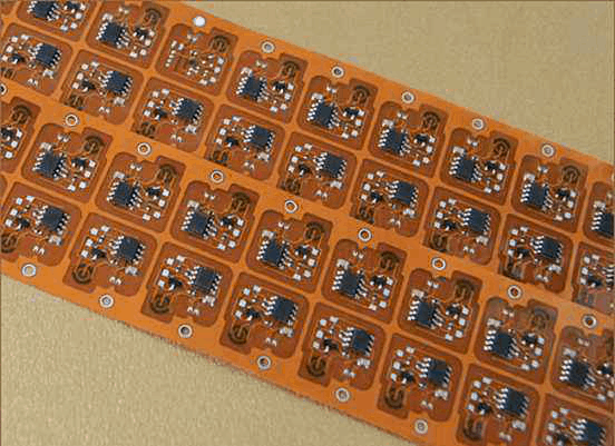
Surface Mount
Overview
Surface mount technology (SMT) involves mounting components directly on the surface of the PCB with their leads or terminals soldered to surface pads. There are no drilled holes required.
Advantages
- Components take up less space on PCB
- Allows placement on both sides of PCB
- Ideal for automated assembly
- Improved system miniaturization
- Typically lower inductance for better high frequency performance
Disadvantages
- Weaker mechanical connection to PCB
- More difficult solder joint inspection
- Requires accurate pick and place equipment
- Not easy to manually solder or modify
Applications
- Low cost high volume consumer electronics
- Modern desktop computing systems
- Cell phones, tablets, and other portable devices
- IoT and embedded systems requiring small form factors
Press-Fit
Overview
Press-fit PCB mounting uses spring-loaded pins that are pressed into plated holes on the PCB to form an interference fit. This creates mechanical attachment without soldering.
Advantages
- Allows components to be attached and detached from PCB multiple times
- Eliminates soldering assembly step
- Enables replacement of individual components
- Good for high temperature operation
Disadvantages
- Requires very precise hole drilling
- Only provides electrical connectivity, no mechanical bond
- Not suitable for high-vibration environments
- Press-fit pins take up space on components
Applications
- Prototyping and low volume production
- Telecom infrastructure where modularity needed
- Large LED display boards that require LED replacement
- Automotive electronics where reworkability is necessary
Screw Terminal
Overview
Screw terminal blocks allow wires to be securely fastened using mechanical screws. The blocks mount directly to the PCB.
Advantages
- Easy to connect and disconnect wires
- Allows quick prototyping changes
- Simple visual inspection of connections
- No soldering required
Disadvantages
- Only suited for prototype or very low volume production
- Takes up significant space on PCB
- No automated assembly
- Not secure enough for critical connections
Applications
- Prototypes
- Education/DIY electronics projects
- Electrical control panels where rewiring is frequent
- Low volume industrial equipment
Soldered Wire
Overview
Wires can be directly soldered to PCB pads, holes, or component leads to form a mechanical and electrical connection.
Advantages
- Very quick and flexible
- Useful for connecting external components or modules
- Allows late-stage modifications
Disadvantages
- Weak mechanism connection prone to failure from vibration or flexing
- No automated assembly
- Time consuming manual process for more than a few wires
- Messy appearance
- Not suitable for production
Applications
- Prototyping
- Education/DIY projects
- Field repairs or modifications
Clip Mounts
Overview
Clip mounting utilizes plastic or metal clips to secure components mechanically. Electrical connection is made via separate soldered wires or pins.
Advantages
- Allows easy component insertion/removal
- Useful for large components like transformers or heat sinks
- Adjustable orientation/positioning
Disadvantages
- Requires additional soldering or cabling
- Less secure electrical connection
- Clips take up space around components
Applications
- Prototyping
- Low volume production where interchangeability needed
- Larger power components like transformers
Adhesive Mounting
Overview
Adhesives and tapes can be used to mechanically fasten components to a PCB surface while wires or pins provide electrical connections.
Advantages
- Simple way to temporarily or semi-permanently mount components
- Allows mounting odd-shaped components
- Good for rapid prototyping
Disadvantages
- Adhesives may fail due to temperature or chemical exposure
- Component rework or removal can be difficult
- Only provides mechanical attachment
- Height limits for some surface mount components
Applications
- Prototyping
- Small run manufacturing where automated pick/place not available
- Education/DIY electronics projects
Solderless Breadboards
Overview
Solderless breadboards have an array of holes and binding posts to allow components to be mechanically inserted and electrically connected without soldering.
Advantages
- Extremely fast to prototype circuits
- Easy component insertion and removal
- Reusable for many iterations
Disadvantages
- Limited connectivity options
- Not very rugged or vibration resistant
- Only suited to low frequency, low power operation
Applications
- Education and prototyping simple circuits
- Verifying circuit operation before designing PCB
- Building temporary circuits with microcontrollers or ICs
Pin Headers
Overview
Pin headers provide an array of male pins that mate with corresponding female sockets. No soldering is required to attach components.
Advantages
- Allows components to be easily plugged/unplugged from PCB
- Useful for modular designed systems
- Permits board stacking expandability
- Components can be mounted on either side of PCB
Disadvantages
- Not as rugged or permanent as soldered connection
- Exposed pins can short if not insulated properly
- Spacing limitations based on header footprint
Applications
- Prototyping circuits on perfboards or breadboards
- Education/DIY projects where modularity is desired
- Stackable embedded systems like Raspberry Pi
- Plug-in modules or daughterboards
Common PCB Mount Considerations
Several factors should be evaluated when selecting a PCB mount methodology:
- Production Volume – High volume automated production favors surface mount while lower volumes allow through-hole or press-fit.
- Vibration/Shock Resistance – Through-hole and some press-fits provide the most rugged mechanical connection to PCB.
- Thermal Considerations – Press-fits or solderless methods avoid heat during assembly.
- Reparability – Press-fit, screw terminal and other non-permanent mounts allow easier field servicing and component replacement.
- Design Iterations – Solderless breadboards, pin headers, screw terminals speed up prototyping changes.
- Assembly Method – Production assembly favors surface mount while prototyping may use solderless or press-fit. Screw terminals allow field wiring changes.
- Component Size – Large or heavy components may require screw down clamp mounts while smaller parts can use adhesive.
- Environment – Vibration resistance requires through-hole or press-fit while moisture or chemical resistance favors conformal coating.
- PCB Real Estate – Surface mount consumes least area while through-hole and some press-fits require more space.
- Performance – Surface mount provides better high frequency and low inductance performance.
Selecting the optimal PCB component mounting method requires balancing these tradeoffs for the specific application. As standards and technologies improve, PCB mount styles continue to evolve offering expanded options to electronics designers.
PCB Mounting Methods Comparison Table
| Method | Soldering Required | Component Removal | Automation Assembly | Ruggedness | Reparability | PCB Space Used |
|---|---|---|---|---|---|---|
| Through-Hole | Yes | Difficult | Hard | Excellent | Moderate | High |
| Surface Mount | Yes | Very Difficult | Excellent | Good | Low | Very Low |
| Press-Fit | No | Moderate | Limited | Moderate | Excellent | Moderate |
| Screw Terminal | No | Very Easy | None | Low | Excellent | High |
| Soldered Wire | Yes | Difficult | None | Low | Moderate | Low |
| Clip | Optional | Easy | Limited | Moderate | Excellent | Moderate |
| Adhesive | No | Moderate | None | Low | Low | Very Low |
| Solderless Breadboard | No | Very Easy | None | Low | Excellent | High |
| Pin Header | No | Easy | Moderate | Moderate | Excellent | Low |
PCB Mounting Methods and Compatible Components
The type of component being mounted also factors into selecting an appropriate PCB attachment method:
- Through-hole – Well suited for large transformers, power terminals, connectors, and legacy components with long leads.
- Surface Mount – Almost all modern low and medium power integrated circuits, transistors, diodes, resistors, and capacitors are available in surface mount packages. Extremely tiny components can only be made as SMDs.
- Press-fit – Press-fit mounts are available for many DIP ICs, LEDs, some connectors, and discreet components like resistors and capacitors.
- Screw terminal – Any component with wire leads can be terminated at a screw terminal. Often used for connecting larger wires.
- Soldered wire – Virtually any component can be soldered to, though best for external modules or flying leads.
- Clip – Useful for large transformers, heat sinks, and tall components requiring mechanical stability.
- Adhesive – Well suited for odd shaped cases, sensors, small microcontrollers, and delicate components.
- Solderless breadboard – Can accept any component with 0.1″ lead spacing like DIP ICs, LEDs, buttons, and passive components.
- Pin header – Most components with a matching pin spacing can be mounted on header, including ICs, connectors, modules, and small circuit boards.
Summary of Major PCB Mount Types
- Through-hole remains a tried and true mounting method, providing excellent mechanical connection for medium/large components not requiring ultra-high density. It allows easy visual inspection and manual solder rework when needed.
- Surface mount has become the standard for high volume commercial electronics, maximizing density and enabling miniaturization. Automated pick and place and reflow soldering allows fast low cost manufacturing.
- Press-fit eliminates soldering while still achieving moderate production volumes. It enables maintenance and upgrades not feasible with soldered parts. The components must be specifically designed for press-fit use.
- Terminal blocks provide convenient termination points for connecting external wires and cables. They allow field servicing without desoldering components. Space requirements limit them to low density applications.
- Solderless breadboards are unmatched for rapidly prototyping circuits and verifying their operation before designing a permanent PCB. While lacking ruggedness, they permit almost infinite reconfigurations.
There is no single “best” PCB mount type applicable to all applications. The environment, production volume, component selection, assembly methods, serviceability needs and other factors dictate the optimal mounting choice for a given design.
PCB Component Mounting Steps
The general procedure for mounting and securing components to a PCB consists of:
1. PCB Design and Layout
- Determine mount technologies compatible with chosen components
- Provide appropriate land patterns for each mounting type
- Include any required holes, pads, or mechanical features
2. PCB Fabrication
- Drill holes for through-hole components if needed
- Ensure pad and land sizes match component footprints
- Plate through-holes or press-fit pads if necessary
- Apply solder mask and silkscreen markings
3. Stencil and Paste Application
- For SMT parts, laser cut stencil with openings for each pad
- Apply solder paste to PCB through stencil openings
4. Component Placement
- Place components mechanically onto board
- For SMT parts use pick and place machine or tweezers
- Press-fit components inserted by hand or fixture
- For through-hole parts, insert leads
5. Soldering
- Reflow solder paste to attach SMT components
- Wave or selective soldering for through-hole parts
- For press-fit avoid soldering if possible
6. Cleaning and Inspection
- Wash away flux residue if reflow soldered
- Visually inspect for missing or faulty connections
- Repair any defects found
7. Conformal Coating (optional)
- Apply protective resin coat to prevent environmental damage
- Useful for high vibration or challenging operating conditions
Proper component mounting is critical during PCB manufacturing and assembly. The mounting style must also be factored in during the design process through appropriate component footprints and land patterns.
Common SMT Footprints
The below footprints are commonly used with surface mount components. The dimensions vary based on component size and pitch:
Two Terminals
- 0402 – Metric size of 0.4mm x 0.2mm
- 0603 – Metric size of 0.6mm x 0.3mm
- 0805 – Metric size of 0.8mm x 0.5mm
- 1206 – Metric size of 1.2mm x 0.6mm
- 1210 – Metric size of 1.2mm x 1.0mm
Four Terminals
- SOIC – Small outline IC package
- QFP – Quad flat pack
- DPAK – Plastic transistor or diode package
- DFN – Dual flat no-lead package
More Terminals
- BGA – Ball grid array package with ball terminals
- LQFP – Low profile QFP package
- TQFP – Thin profile QFP
- PGA – Pin grid array
The PCB land patterns for these footprints match the component terminal layouts and sizes. High density mounting requires smaller SMT packages and 0.5mm pitch or less.
SMT Assembly Methods
Surface mount components are assembled to PCBs using either:
Reflow Soldering
- Solder paste applied through stencil
- Components placed with pick/place machine
- Board heated in oven profile to reflow solder
Wave Soldering
- Bottom side components glued in place
- PCB passed over flowing wave of solder
- Solder adheres to component pads
Hand Assembly
- Components held in place with adhesive or tape
- Solder paste applied manually
- Carefully soldered by hand with iron
Reflow soldering is ideal for high volume production while hand assembly supports low volume or rework. Wave soldering is best for high mix/low volume.
Press-Fit Assembly
Press-fit component installation involves:
- PCB with plated through holes at component locations
- Components with spring pins inserted by hand or fixture
- Pins compress slightly to grip hole walls securely
- Allows easy insertion and removal
No soldering is required since the spring pins make electrical contact. Mechanical support may be needed for heavier components. Press-fit provides a good balance between field reworkability and production automation.
Through-Hole Component Installation
Through-hole parts are mechanically assembled by:
- Inserting component leads/wires into corresponding PCB holes
- Bending leads slightly to hold component in place
- Clipping excess lead length if necessary
- Turning board upside down to solder
- Flowing solder into joints til fillet forms around hole
Axial leaded components like resistors, diodes, capacitors, and inductors are easily inserted by hand or with automated placers. Components with many pins may utilize machined pin insertion guides.
Common PCB Component Fasteners
In addition to soldering, components can be mechanically secured to PCBs using:
Screws
- Pass through mounting holes and fasten with nut
- Permit easy component access or replacement
- Must allow room for fastener hardware
Standoffs
- Threaded spacers soldered to board
- Components attached on top with screws
- Provides secure connection with access underneath
Clips
- Snaps onto edge of PCB or component
- Holds parts in place without soldering
- Different styles for various size components
Adhesives
- Small dab of glue applied to hold component
- Epoxy for very strong permanent bond
- Removable tapes can allow repositioning
These methods help ensure components are physically secured to the PCB in demanding environments.
PCB Mounting Hole, Slot, and Cutout Guidelines
In addition to pads and traces, PCB layouts often require:
Mounting Holes
- Located where screws will attach board to enclosure
- Should have sufficient annular ring width for solder mask
- May need wider clearance cutouts


Leave a Reply