Introduction
Determining appropriate trace widths is an essential part of printed circuit board (PCB) design. Trace width has a major impact on current carrying capability, voltage drop, thermal performance, signal quality, and manufacturability.
This guide will provide a comprehensive overview of how to calculate optimal PCB trace widths using manual calculations and PCB design software. We’ll examine the key factors involved, trace width equations, how to use trace width calculators, and trace width best practices.
By the end, you’ll understand the core considerations in choosing trace widths, be able to perform the necessary calculations, and make trace routing decisions optimized for your designs. Properly selecting trace dimensions ensures your boards function and perform reliably.
What is PCB Trace Width?
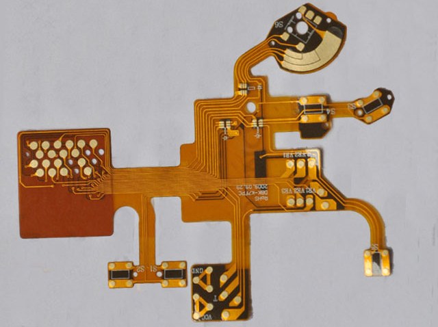
Trace width refers to the width of the copper tracks on a printed circuit board that carry signals and power between different components and pins. Trace widths typically range from under 0.2 mm up to several millimeters.
Some key terms:
- Traces – The conductive copper pathways on a PCB.
- Tracks – Another term for copper traces.
- Trace Width – The width dimension of a trace (typical units are mils or mm).
- Trace Thickness – The height of the copper layer (typically 0.5 to 2 oz).
Choosing suitable trace widths is essential for managing current capacity, impedance, signal quality, manufacturability, and cost. Let’s look at how to calculate appropriate widths.
Factors That Determine Trace Width
Several considerations must be taken into account when selecting PCB trace widths:
Current Carrying Capacity
Wider traces can handle higher current loads without overheating. Thinner traces may exceed temperature limits.
Voltage Drop
Thicker traces reduce unwanted voltage drop across the track. Thin, high current traces drop more voltage.
Impedance Control
Controlled impedance traces require widths calculated to achieve target impedance, based on layer height and dielectric constant.
Signal Quality
Thinner traces are more susceptible to interference and noise pick up. Wider traces maintain better signal integrity.
Manufacturing Constraints
PCB fab has minimum trace/space rules. Very thin traces may be outside capabilities.
Routing Congestion
Available space Determines feasible widths. Dense designs need thinner traces to route.
Cost
Narrower traces use less copper area, reducing manufacturing cost. But too thin risks reliability.
We’ll now examine how to quantify these considerations into an optimal trace width.
Trace Width Calculations
There are two main methods of calculating appropriate PCB trace widths:
1. Manual Calculations
Use equations to compute suitable width based on current, temperature rise, and other constraints.
2. Software Calculators
Tools in PCB design software automate width calculations based on user inputs.
Let’s look at both manual and software-based approaches.
Manual Trace Width Calculations
To manually calculate trace widths, key parameters are:
- Current (I) – Amount of current in amps
- Temperature Rise (ΔT) – Allowable increase over ambient
- Copper Thickness (h) – Oz weight of the copper foil
- Copper Conductivity (k) – Based on material, typically 390 W/m°K
- Maximum Ambient Temperature (Ta) – Environment temperature
With these inputs, the core equations are:
1. Calculating Cross Sectional Area
The cross sectional area of the trace accounts for its thickness. This is needed to find current density.
Cross Section Area = Trace Thickness x Trace Width
A = h x w
2. Finding Current Density
Current density is current per unit cross sectional area. This is used to calculate temperature rise.
Current Density = Current / Cross Sectional Area
J = I / A
3. Calculating Temperature Increase
Using the current density, the temperature rise equation is:
ΔT = (J2 x Electrical Resistivity) / Thermal Conductivity
Where electrical resistivity is 1/conductivity:
ΔT = (J2 x 1/k) / k
4. Applying Temperature Limit
With the ΔT found, the trace width is calculated to hold the temp rise within specified ambient limits:
Maximum Temperature = Ambient Temp + Temperature Rise
Ta = Ta + ΔT
This manual calculation provides the minimum trace width to keep temperature within set limits at the designed operating current.
While conceptually straightforward, manual calculations can become tedious with many traces. This is where software trace width calculators simplify the process.
Using PCB Software Trace Width Calculators
To automate trace width determination, PCB design tools like Altium Designer, Eagle, and KiCad include built-in calculators that provide the width after entering key parameters.
The workflow is:
1. Enter Parameters
- Current, copper weight, temp rise, ambient temp
2. Select Internal/External
- Inside board or open air
3. Specify Layers
- Single, internal, external
4. Set Calculation Standard
- IPC-2221 or other spec
5. Run Calculator
- Tool computes minimum width
6. Apply Width to Routing
- Set trace width rule based on result
This greatly simplifies determining valid widths compared to manual calculations. The software handles all the underlying equations automatically.
Trace Width Guidance for Common Conditions
Here are some typical trace width guidelines:
- Low power logic – 10-15 mils
- Modal logic – 15-25 mils
- High power logic – 25-40 mils
- Power traces – 40+ mils
- USB 2.0 – 8-10 mils (90 ohm differential impedance)
- PCI Express – 5-8 mils (100 ohm differential)
- DDR3 Memory – 5-6 mils width, 11-12 mils spacing
These provide reasonable starting points for refinement based on detailed calculations.
Trace Width Design Tips
Here are some best practices when planning PCB trace widths:
- Size widths based on maximum expected current draw
- Account for temperature derating and ambient conditions
- Use thicker copper layers for better current capacity
- Minimize length of high current traces
- Avoid excessive or pure 90 degree bends
- Utilize solder masks defined traces where possible
- Set wider widths for power traces vs signal traces
Following these guidelines will help maximize performance and reliability.
Trace Width Effects on Manufacturing
Trace width also impacts PCB manufacturing:
- Thinner widths allow routing complex designs but increase fabrication cost
- Small widths and spaces challenge fabrication tolerances
- Very thick traces use more copper and can cause etching issues
- Defining minimum width/space rules ensures manufacturability
Assessing manufacturing capabilities relative to trace dimensions is prudent before finalizing board layout.
Conclusion
Calculating optimal trace widths requires considering current flow, voltage drop, temperature rise, signal integrity and manufacturability constraints.
Manual computations based on cross section and current provide a basic width value. More advanced formulas account for other factors.
PCB design software trace width calculators simplify the process by handling computations automatically after entering key parameters.
Combining width calculations with practical width guidelines, design tips, and fabrication feedback results in a trace routing strategy tailored for your specific design needs.
Properly sized trace widths form the foundation of functional, high performing, reliable PCBs.
Frequently Asked Questions
How are trace widths calculated manually?
Manually trace widths can be calculated using the cross sectional area, current density based on current flow, and temperature increase based on the heat generated in the trace. This provides the minimum width to stay within temperature limits.
What is a typical PCB trace width?
Typical PCB trace widths for common signals are:
- Power traces: >50 mils
- Low speed logic: 10-20 mils
- High speed logic: 25-35 mils
- DDR SDRAM: 5-8 mils width, >10 mils spacing
So widths span a large range based on current, voltages, and type of signals being routed.
What PCB trace width should I use?
Choosing PCB trace width depends on the signals being routed. Some guidelines:
- Power traces: Use thick >50mil traces
- Digital logic: 15-30 mils, match impedance
- Analog signals: >20mils, ensure lower impedance
- High speed buses: Match trace width to specified differential impedance
How accurate are PCB trace width calculators?
PCB calculator tools provide a reasonably accurate starting point for trace widths as long as the key parameters of current, copper thickness, temp rise and ambient temp are entered correctly. But the width should still be refined through analysis and review.
What impacts PCB trace width?
The main factors impacting trace width design are current flow, voltage drop, temperature rise, impedance requirements, signal quality needs, noise susceptibility, manufacturability rules, and routing congestion constraints. Accounting for these effects results in an optimal width.


Leave a Reply