Introduction
A PCB or printed circuit board assembly refers to the complete assembled PCB after all components have been soldered onto the bare PCB. This guide will provide a full overview of PCB assemblies including their purpose, components, design considerations, manufacturing process, testing requirements and applications across different industries.
We’ll examine the key steps involved in creating a functional PCB assembly from fabrication and population to final testing. Whether you’re looking to have PCB assemblies made or simply want to understand what goes into producing a fully assembled board, this article will cover all the essential information.
By the end, you’ll have a comprehensive understanding of PCB assemblies and how they deliver connectivity, processing, sensing, controls, human interfaces and other functionality at the heart of electronics.
What is a Bare PCB?
To understand what constitutes a PCB assembly, it’s helpful to first distinguish between a bare PCB and a populated PCB assembly.
A bare printed circuit board refers to the base board after fabrication but before any components are mounted. This consists of:
- Substrate – Usually FR-4 fiberglass epoxy laminate
- Copper traces – Forms the conductive pathways
- Pads/lands – Exposed copper areas for soldering
- Silkscreen – Markings for components, text, logos
- Soldermask – Epoxy coating exposing only pads
This bare PCB provides the foundation. The board assembly process takes this base and solders on all the necessary components like ICs, resistors, connectors etc to create a functional PCB assembly.
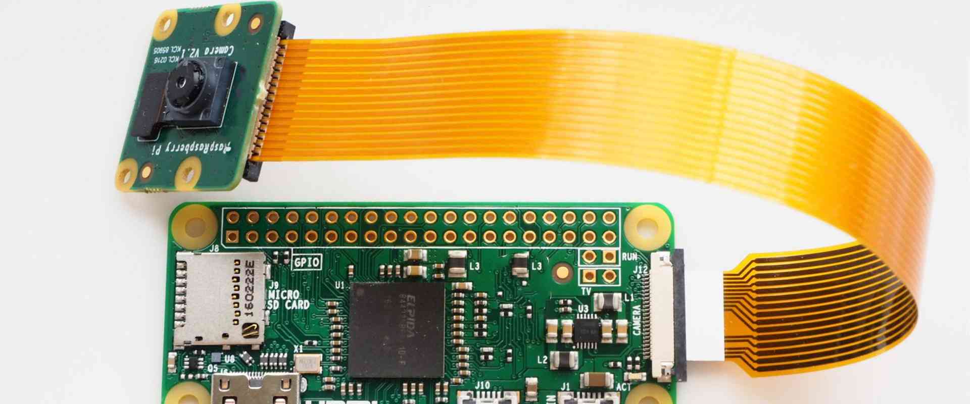
What is a PCB Assembly?
A PCB assembly consists of:
- Bare PCB board
- Mounted and soldered components
- Any hardware like connectors, buttons, displays
- Conformal coating or potting compounds
- Mechanical parts like heatsinks or fasteners
When completely assembled and soldered, these boards provide the same functionality as a printed circuit board within electronic products and devices. PCB assemblies contain all the interconnected electronic components that enable the intended operation.
Some key points about PCB assemblies:
- They realize the electronic circuit design physically
- Enable complex functions in a compact form factor
- Simplify manufacturing and assembly vs. point-to-point wiring
- Standardized platform used across many industries
Let’s now look at the role of PCB assemblies in manufacturing.
PCB Assemblies in Manufacturing Workflows
For any electronic hardware product requiring a circuit board, the manufacturing stages typically involve:
PCB Fabrication
- Create bare PCB based on the design files
PCB Assembly
- Solder components onto bare PCBs
Product Testing
- Test assembled PCBs for quality/performance
Product Assembly
- Install PCB assembly into enclosures with other parts
Final Testing
- Validate functionality of finished product
The PCB assembly stage bridges the fabricated board and the final product assembly to create a functional electronics subsystem.
Understanding this workflow context highlights the importance of PCB assemblies in transforming raw PCB boards into operational hardware ready for integration.
Applications of PCB Assemblies
PCB assemblies provide the electronic functionality across virtually all industries. Some common applications include:
- Consumer electronics – Phones, laptops, peripherals
- Automotive – Engine control units, dashboards, sensors
- Industrial – Motor drives, robotics, test equipment
- Medical – Patient monitors, imaging equipment
- Aerospace – Avionics, guidance systems
- Military/Defense – Radar, communications, navigation
- Telecommunications – Routers, base stations, switches
This list covers just a small sample. PCB assemblies can be found in everything from home appliances and IoT devices to servers and networking infrastructure. They provide application-specific capabilities but all follow a generally standardized assembly process.
Next we’ll take a deeper look at that process and the steps involved in manufacturing completed PCB assemblies.
PCB Assembly Process Overview
The assembly of a populated, functional board from a bare PCB involves three main high-level steps:
1. Component Population
The bare PCB board is populated with all required components like:
- Active components – ICs, microcontrollers, transistors, diodes
- Passive components – Resistors, capacitors, inductors
- Electromechanical – Switches, buttons, sensors
- Connectors and sockets – USB, HDMI, D-SUB, edge connectors etc
- Any other parts – Crystals, oscillators, LEDs, thermistors, fuses
This is done through SMT pick and place machines and/or manual insertion of leaded components.
2. Soldering
Components are soldered for both mechanical attachment and electrical connection.
Types of soldering include:
- Reflow – For surface mount devices
- Wave – For high volume SMT production
- Hand soldering – For through hole parts
3. Post Soldering Processes
Additional steps like:
- Conformal coating for protection
- Hardware assembly
- Programming firmware/software
- Attaching connectors or labels
This completes the board ready for testing and installation into end products.
We’ll now do a deeper dive on each stage.
PCB Assembly Process Steps
The assembly sequence involves precision manufacturing processes to transform bare boards into fully functional PCB assemblies. Here is more detail on each step:
1. Component Population
This involves mounting components onto the fabricated PCB. There are two main methods:
1.1: SMT Pick and Place
Uses machines to precisely place surface mount devices (SMDs, SMT) onto PCB pads. Feeders or tapes provide components which are picked and positioned by the head onto solder paste.
Benefits:
- Very fast and accurate placement
- Ideal for high volume production
- Handles component sizes down to 0201 chips (0.6mm)
1.2: Manual Insertion
Human operators manually insert leaded components like DIP ICs, resistors, TO headers into through holes or solder pads, typically assisted by jigs.
Benefits:
- Allows placement of tall or heavy through hole parts not suitable for pick-and-place
- Lower equipment cost for small volumes or prototypes
For maximum efficiency, SMT parts are mounted first through pick and place, followed by manual insertion of any through hole parts.
2. Soldering
Soldering electrically and mechanically joins components to the PCB by melting solder to form the interconnects between pads and leads/terminations. Common techniques:
2.1: Reflow Soldering
Applies controlled heat (in an oven) to melt paste deposited by pick and place, bonding SMT parts to pads.
Benefits:
- Ideal for high density SMT parts and smaller chips
- Fast process suitable for volume production
- Provides strong, reliable solder joint
2.2: Wave Soldering
Passes bottom side of PCB over a wave of liquid solder to solder all leads simultaneously.
Benefits:
- Very fast process for high volume SMT production
- Lower cost than reflow
Limitations:
- Only solders bottom side of PCB
- Not suitable for small components
2.3: Hand Soldering
Manual soldering of joints by operator, usually for through hole components.
Benefits:
- Allows rework and repair of boards
- Useful for quick prototyping
- Low equipment cost
Limitations:
- Slow process, high labor
- Skill-dependent for quality
The soldering methods are optimized based on production environment and mix of SMT and through hole parts.
3. Post Soldering Processes
Additional steps after soldering to complete PCB assembly:
- Conformal coating – Epoxy layer prevents shorts and adds environmental protection
- Hardware assembly – Attaching brackets, connectors, heat sinks, etc
- Programming – Loading firmware onto microcontrollers
- Inspection – Visual or automated optical inspection (AOI)
- Testing – Power-on testing to validate basic functionality
- Packaging – Bagging or boxing assembled boards for storage and shipment
This finalizes the board assembly process, producing a functional, populated PCB ready for installation and more extensive testing.
Designing for PCB Assembly
To optimize a design for efficient, high-yield assembly, key factors include:
Component Selection
- Prefer standard parts that are readily available
- Minimize component variants to reduce inventory
- Select suitable package sizes (0201 vs 0805 vs 1206 etc)
Placement
- Group related components logically
- Ensure adequate component spacing
- Place for convenient hand assembly access
Solderability
- Include exposed thermal pads if needed
- Provide sufficient pad sizes for leads
- Follow assembly guidelines for BGAs, QFNs etc
- Include test pads connected to key nets
- Allow test probes access
Markings
- Clear polarity markers, component IDs
- Board reference designators
Considering these design-for-assembly (DFA) factors upfront will help avoid issues and minimize assembly time and cost.
Testing PCB Assemblies
Thoroughly testing completed PCB assemblies is crucial before shipment and end product integration. Typical quality control testing includes:
Inspections
- Visual inspection under microscope
- X-ray inspection for hidden defects
- Automated optical inspection (AOI)
Electrical Testing
- Open/shorts detection
- In-circuit testing for component faults
- Flying probe testing of nets/traces
- Boundary scan for digital logic
Function Testing
- Validate against operational requirements
- Environmental stress testing
This combination of inspection, electrical, and functional testing provides comprehensive quality assurance and screens any defective boards. Production test fixtures are often custom designed for each PCB assembly.
Outsourcing vs In-House Assembly
For companies needing PCB assembly services, there are two options:
Outsourced Assembly
- Using a specialized contract manufacturer
- No inventory or equipment costs
- Lower volumes more economical
- Longer lead times on first builds
In-House Assembly
- Full control over process
- Faster turnaround after initial setup
- Higher equipment capex
- Requires trained operators
- Only viable at high volumes
Weighing the pros and cons allows selection of the best service model. Many businesses will prototype through outsourcing but transition internally for higher volume production.
Key Considerations for PCB Assembly
Here are some important factors when dealing with PCB assemblies:
- What mix of SMT and through hole components? Impacts process selection
- How many unique board configurations/BOMs? Adds complexity
- Lowest component pitch/spacing? Could require finer solder mask
- What tolerances needed? High precision increases costs
- Any dense BGAs or connectors requiring x-ray? Adds inspection time
- Number of layers? More layers increases fabrication time and cost
- Any large heat sinks or mechanical hardware? May require hand assembly
- What test coverage needed? More validation increases test complexity
Understanding requirements in terms of part mix, precision, and validation needs allows optimizing the assembly process and estimating costs.
Conclusion
This guide covered the key aspects related to PCB assemblies including:
- The components and materials constituting a PCB assembly
- Where PCB assemblies fit in the electronics manufacturing sequence
- The detailed step-by-step assembly process flow
- Design considerations for efficient assembly
- Testing methods to validate assembled boards
- Factors in deciding between in-house vs outsourced assembly
By understanding what goes into creating and validating a populated PCB assembly, you can make more informed design decisions and select optimal manufacturing approaches tailored to your specific product.
Frequently Asked Questions
What is the difference between PCB fabrication and PCB assembly?
PCB fabrication refers to the manufacturing of the bare board itself. PCB assembly is the process of soldering components onto the fabricated PCB to create a functional electronic circuit.
Are PCB assembly and PCB manufacturing the same thing?
They refer to different stages of the process. PCB manufacturing or fabrication produces just the bare board. PCB assembly populates the bare board with components to create the complete, functional PCB.
What are the components of a PCB assembly?
A PCB assembly consists of the bare board plus mounted components like ICs, resistors, capacitors, connectors, displays, hardware etc. Essentially a PCB assembly contains all the electronic parts which realize the intended circuit functionality.
Does PCB assembly require programming?
Some PCB assemblies will require firmware or embedded software to be loaded onto microcontrollers or other programmable chips on the board as part of the assembly process. This depends on the specific application.
What is the most common assembly process for PCBs?
For medium to high volumes, the most common process is SMT component placement by pick-and-place machine followed by reflow soldering in a convection oven. Through-hole parts can be added manually after reflow. Routing boards over a wave soldering system is another very high volume SMT assembly method.


Leave a Reply