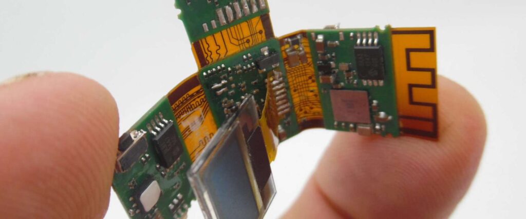
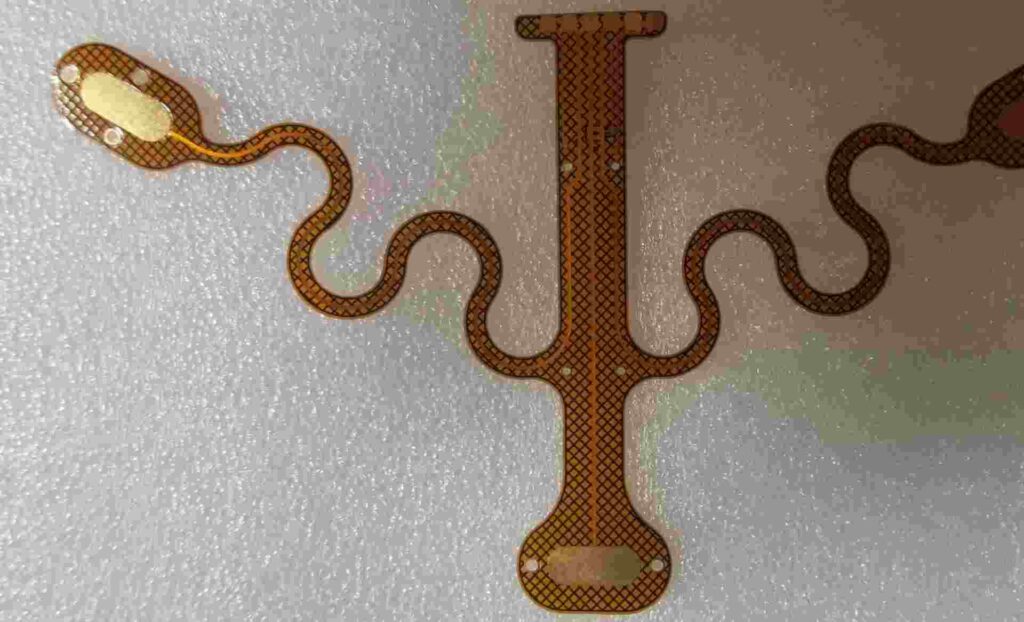
Flexible printed circuit boards (flex PCBs) allow circuitry to bend and flex to fit into tight or dynamic spaces. As electronics become smaller and more complex, flex PCBs have become increasingly popular options. While 2-4 layer flex PCBs meet many needs, advanced applications may require more layers. 8 layer flex PCBs provide more routing channels and greater functionality in a compact form factor. This guide covers everything you need to know about 8 layer flex PCBs.
What are 8 Layer Flex PCBs?

A flex PCB is made of flexible dielectric layers laminated together with conductive traces in between. The number of conductive layers determines the number of layers in the flex PCB. An 8 layer flex PCB contains 8 layers of circuitry.
Here is the basic layer stackup:
- Layer 1 – Bottom conductive layer
- Layer 2 – Dielectric
- Layer 3 – Conductive layer
- Layer 4 – Dielectric
- Layer 5 – Conductive layer
- Layer 6 – Dielectric
- Layer 7 – Conductive layer
- Layer 8 – Top protective coverlay
With 8 routing layers, these PCBs can integrate more complex circuits and components in a smaller space than lower layer count boards. The flexing capability allows the board to bend around corners or moving parts.
8 layer flex PCBs provide the following advantages:
- More routing channels – Up to 8x the routing channels versus 2 layer flex.
- Higher component density – Fit more components and complexity.
- Miniaturization – Achieve smaller, lighter, and more compact circuits.
- Dynamic flexing – Bend and flex to fit tight spaces and moving parts.
- Noise isolation – Additional layers help isolate noisy signals.
- Impedance control – Extra layers provide more control over impedance.
- Shielding – Ground planes shield sensitive signals from interference.
- Mixed signal – Integrate digital and analog signals.
- High speed – Supports high frequency signals up to GHz range.
When to Use 8 Layer Flex PCBs
Here are some examples of when 8 layer flex PCBs may be suitable:
Advanced Wearable Devices
Wearable medical devices, fitness trackers, smart watches, and augmented reality headsets require compact, dynamic, and complex circuitry. The tight space constraints make 8 layer flex PCBs a good fit. The flexing enables the PCB to move with the body.
Automotive Applications
Automotive sensors, cameras, lighting, engine controls, and in-vehicle infotainment have stringent size and reliability requirements. 8 layer flex PCBs allow automotive electronics to fit into tight spaces while withstanding vibration.
Consumer Electronics
Phones, laptops, and tablets continue to get thinner and lighter. Using 8 layer flex PCBs helps squeeze more functionality into less space in these increasingly compact consumer electronics.
Aerospace and Defense
Avionics, guidance systems, and satellites need reliable, high density PCBs that can withstand intense vibration, shock, and temperature changes experienced during launch and flight.
Medical Devices
Medical devices like endoscopes, hearing aids, and implantables are extremely space constrained. 8 layer flex PCBs can integrate the necessary functionality while conforming to tight shape requirements.
Robotics
Robotic systems demand complex circuitry that can flex and move. 8 layer flex PCBs bring together high component density, dynamic bending, and ruggedness needed in robotics.
In summary, 8 layer flex PCBs should be considered when an application requires:
- Extremely compact, complex circuitry
- Ability to conform to tight, dynamic spaces
- Signal integrity at high frequencies
- Miniaturization and weight reduction
- Reliability under shock, vibration, flexing
Design Considerations
Designing an 8 layer flex PCB requires special considerations for routability, layer stackup, and bend radius.
Routability
With 8 routing layers, sufficient vertical spacing is needed between traces and components on different layers to prevent shorts. This requires careful board layout practices.
- Use larger component packages when possible.
- Group components on the same side of the board when feasible.
- Leave adequate spacing around drilled holes.
- Utilize manufacturers design for manufacturing (DFM) checks.
- Work closely with PCB designers experienced in complex multilayer boards.
Layer Stackup
The designer must determine optimal layer stackup – the arrangement of dielectric, adhesive, and copper layers. Important factors include:
- Which layers are signal layers vs. ground/power planes
- Signal layer pairing to control impedance
- Dielectric materials and thicknesses
- Plane placement for shielding and noise isolation
- Optimizing stackup for manufacturability
The stackup must be engineered to meet electrical, mechanical, and manufacturability requirements. Signal integrity modeling and simulations should be used to verify the stackup design.
Bend Radius
Flex PCBs must be designed with proper bend radius to prevent damage. The minimum bend radius is determined by:
- Board thickness
- Copper thickness
- Dielectric material
- Number of layers
In general, a minimum inside bend radius over 3x the total board thickness should be used. But the radius should ultimately be verified through physical testing and with manufacturer guidance.
Materials and Construction

8 layer flex PCBs leverage specialized materials and fabrication processes.
Dielectrics
Polyimide is most commonly used due to its excellent flexibility, temperature resistance, and chemical resistance. Other options include PEN, PET, polyester, and fluoropolymers. Thin dielectrics help maximize flexibility.
Adhesives
Flexible acrylic, epoxy, or polyimide adhesives bond the layers together. They must withstand flexing without delamination.
Copper
Rolled annealed copper foils are typically used, but very thin copper down to 12 micron may be used to optimize flexibility.
Coverlay
The top and bottom layers are covered with a protective flexible coverlay material like polyimide. Coverlay openings expose solder pads.
Vias
Microvias with diameters below 0.15mm are used to connect between layers. Vias are staggered when possible to improve reliability under dynamic flexing.
Stiffeners
Strategically placed stiffeners made of thicker dielectric layers or metal areas help control flexing in certain regions.
Solder Mask
LPI solder mask withstands flexing and protects traces from environmental exposure.
Manufacturing Process
8 layer flex PCBs demand tight process controls to ensure quality. Here is a general manufacturing workflow:
- CAM and Engineering – Engineers review board stackup, trace routing, plane design, layer alignment, etc. and create manufacturing data.
- Inner Layer Fabrication – Dry film photoresist lamination, exposing, developing, and etching creates the inner circuit layers.
- Lamination – Layers are precisely aligned and laminated together under heat and pressure.
- Drilling – A precision mechanical or laser drill creates the through holes and microvias.
- Metallization – Walls of drilled holes are plated with copper to form electrical connections between layers.
- Outer Layer Fabrication – Same photolithography process used to pattern the outer circuit layers.
- Solder Mask – LPI solder mask is laminated and patterned to expose solder pads.
- Legend Printing – Solder mask openings are printed with component identifiers.
- Route and Test – Boards are routed into individual PCBs, electrically tested, and inspected.
- Shipping – boards are shipped to customers.
Rigorous quality control is implemented throughout the process. Automated optical inspection, electrical testing, cross-section analysis, and surface roughness measurements identify any defects.
Quality and Reliability
Producing reliable, high yielding 8 layer flex PCBs requires an experienced manufacturer with proven qualifications. Here are key reliability considerations:
Materials and Construction
- Materials like polyimide dielectric properly selected
- Adhesives prevent delamination under dynamic flexing
- Thieving techniques ensure uniform copper distribution
- Plating quality prevents cracks or lifting
Modeling and Testing
- Simulation used to model stresses and optimize design
- Test vehicles validate minimum bend radius
- HAST, temperature cycling, and vibration testing
Process Controls
- Automated optical inspection of inner and outer layers
- Tight layer alignment tolerances
- Drilling meets hole size and placement precision requirements
- Systematic process monitoring at each step
- Lot traceability through entire fabrication
A rigorous qualification process including design reviews, material evaluations, test vehicle builds, product testing, facility audits, and more should give confidence in consistent quality and reliability.
Summary of Key Benefits
- Complex routing in a very small form factor
- Ability to integrate sensitive analog and high speed digital signals
- High component density with up to 8x more routing channels
- Thin, lightweight, and dynamic flexing capability
- Noise isolation through multiple ground planes
- Robust support of high frequency signals
- Reliable construction with advanced materials like polyimide
- Proven capability to meet miniaturization and reliability requirements of advanced flex PCB applications
For products where complexity, density, signal integrity, and compact construction are critical, 8 layer flex PCBs provide an enabling solution.
Frequently Asked Questions
What are typical minimum feature sizes and spacing for 8 layer flex PCBs?
The minimum trace width and spacing is typically around 100 micron (4 mils). But advanced processes can achieve smaller minimum features down to 50 micron (2 mil) trace/space. Microvias with 8-10 mil diameter can be reliably produced.
What are the typical dielectric materials used?
Polyimide is the most common dielectric for flex PCBs, but others like PEN, PET, and polyester may also be used. Dielectric thicknesses generally range from 12-100 micron. Thinner dielectric improves flexibility.
What are considerations for controlled impedance on 8 layer flex PCBs?
Controlling impedance requires careful stackup design, proper dielectric materials, tight thickness tolerances, and use of closely coupled signal layer pairs. Wider traces are often required verses rigid boards. Simulations and test coupons validate impedance control.
How small can an 8 layer flex PCB be reliably produced?
Flex PCBs under 0.5mm total thickness can be challenging in an 8 layer stackup due to signal integrity and manufacturability concerns. Most applications aim for 0.8mm total thickness as a practical minimum.
Can stiffeners and solder mask be used to control flexing?
Yes, strategically placed stiffeners and solder mask can “lock down” certain regions to control the flex radius and prevent overflexing of sensitive components. The stiffeners can be implemented with thicker dielectric or additional copper.
How are 8 layer flex PCBs tested?
Testing focuses on electrical connectivity and continuity between layers, verification of insulation resistance, and examination of physical defects under magnification. Environmental stress testing like thermal cycling, vibration, and bend testing help validate robustness. Test coupons can provide design feedback.
Conclusion
As products require continued miniaturization and circuit complexity, 8 layer flex PCB technology provides an enabling solution. With up to 8 routing layers folded into a thin, bendable package, flex PCBs can integrate a tremendous amount of circuitry while conforming to the tightest space constraints and dynamic flexing requirements.
Advanced materials like polyimide dielectric and flexible adhesives ensure robust performance under harsh conditions. Careful stackup design and tight process controls at all manufacturing stages result in reliable multilayer flex circuits. For medical, consumer, automotive, aerospace, and defense applications pushing the boundaries, 8 layer flex PCBs deliver proven performance in a highly compact form factor.


Leave a Reply