Introduction to the 74LS76
The 74LS76 is part of the 7400 series of TTL (Transistor-Transistor Logic) ICs. It contains two independent J-K flip-flops with preset and clear inputs. Each flip-flop has two outputs: Q and its complement Q’. The IC is widely used in various digital circuits, such as counters, shift registers, and synchronous logic designs.
Key Features of the 74LS76
- Dual J-K flip-flops in a single package
- Preset and clear inputs for each flip-flop
- TTL-compatible inputs and outputs
- High speed operation
- Low power consumption
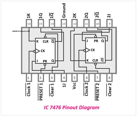
74ls76 pinout Diagram
To understand the functionality of the 74LS76, it is crucial to familiarize yourself with its pinout. The following table shows the pin assignments for the 74LS76 in a 16-pin DIP (Dual Inline Package) format:
| Pin Number | Pin Name | Description |
|---|---|---|
| 1 | 1CLK | Clock input for flip-flop 1 |
| 2 | 1J | J input for flip-flop 1 |
| 3 | 1K | K input for flip-flop 1 |
| 4 | 1PRE | Preset input for flip-flop 1 (active low) |
| 5 | 1CLR | Clear input for flip-flop 1 (active low) |
| 6 | 1Q | Q output for flip-flop 1 |
| 7 | 1Q’ | Q’ output for flip-flop 1 (complement of Q) |
| 8 | GND | Ground |
| 9 | 2Q’ | Q’ output for flip-flop 2 (complement of Q) |
| 10 | 2Q | Q output for flip-flop 2 |
| 11 | 2CLR | Clear input for flip-flop 2 (active low) |
| 12 | 2PRE | Preset input for flip-flop 2 (active low) |
| 13 | 2K | K input for flip-flop 2 |
| 14 | 2J | J input for flip-flop 2 |
| 15 | 2CLK | Clock input for flip-flop 2 |
| 16 | VCC | Power supply (+5V) |

Understanding the J-K Flip-Flop
The 74LS76 contains two J-K flip-flops, which are the building blocks for various digital circuits. A J-K flip-flop has two inputs (J and K) and two outputs (Q and Q’). The behavior of the flip-flop depends on the states of the J and K inputs at the rising edge of the clock signal.
Truth Table for J-K Flip-Flop
| J | K | Q(t+1) |
|---|---|---|
| 0 | 0 | Q(t) |
| 0 | 1 | 0 |
| 1 | 0 | 1 |
| 1 | 1 | Q'(t) |
In the truth table above, Q(t) represents the current state of the flip-flop, while Q(t+1) represents the next state after the rising edge of the clock signal.
Preset and Clear Inputs
The 74LS76 also features preset (PRE) and clear (CLR) inputs for each flip-flop. These inputs are active low, meaning that when they are connected to a logic ‘0’ (ground), they override the J and K inputs and force the flip-flop to a specific state.
- When PRE is set to ‘0’, the flip-flop is set to ‘1’ (Q = 1, Q’ = 0), regardless of the J and K inputs.
- When CLR is set to ‘0’, the flip-flop is reset to ‘0’ (Q = 0, Q’ = 1), regardless of the J and K inputs.
If both PRE and CLR are set to ‘0’ simultaneously, the behavior of the flip-flop is undefined.

Applications of the 74LS76
The 74LS76 finds its use in various digital circuits and applications. Some common examples include:
Counters
The 74LS76 can be used to create synchronous counters by cascading multiple flip-flops. By connecting the Q output of one flip-flop to the clock input of the next flip-flop, you can create binary counters, BCD counters, or custom counting sequences.
Shift Registers
J-K flip-flops can be used to construct shift registers, which are essential components in serial data transmission and storage. By connecting the Q output of one flip-flop to the J input of the next flip-flop, you can create a serial-in, serial-out (SISO) shift register.
State Machines
The 74LS76 can be used to implement state machines, which are sequential logic circuits that transition between different states based on input conditions. By designing the appropriate combinational logic and feedback paths, you can create Mealy or Moore state machines using J-K flip-flops.

Interfacing with the 74LS76
When working with the 74LS76, it is essential to ensure proper interfacing with other components in your circuit. Here are some guidelines to follow:
Power Supply
The 74LS76 requires a stable +5V power supply connected to the VCC pin (pin 16). The GND pin (pin 8) should be connected to the common ground of your circuit.
Input Signals
The input signals to the 74LS76 should be TTL-compatible, meaning that they should have voltage levels of approximately 0V for logic ‘0’ and +5V for logic ‘1’. Ensure that the input signals meet the required voltage thresholds and have clean transitions to avoid unwanted behavior.
Output Loading
The outputs of the 74LS76 can drive a limited amount of current. When connecting the outputs to other components, make sure not to exceed the maximum output current rating specified in the datasheet. If you need to drive high-current loads, consider using buffer ICs or transistor drivers.
Troubleshooting Tips
If you encounter issues while working with the 74LS76, consider the following troubleshooting tips:
- Double-check the pinout connections to ensure that all pins are properly connected to the appropriate signals and power supply.
- Verify that the input signals meet the required voltage levels and have clean transitions.
- Check for any short circuits or open connections in your circuit that may affect the behavior of the flip-flops.
- Use an oscilloscope or logic analyzer to observe the waveforms at different points in your circuit and compare them with the expected behavior.
Frequently Asked Questions (FAQ)
-
What is the difference between the 74LS76 and other J-K flip-flops?
The 74LS76 is a dual J-K flip-flop, meaning it contains two independent flip-flops in a single package. It also features preset and clear inputs for each flip-flop, which allow you to force the outputs to a specific state. -
Can I use the 74LS76 with a 3.3V power supply?
No, the 74LS76 is designed to operate with a 5V power supply. Using a lower voltage may result in unreliable operation or damage to the IC. -
How do I create a toggle flip-flop using the 74LS76?
To create a toggle flip-flop, connect the Q’ output to both the J and K inputs of the same flip-flop. This configuration will cause the output to toggle between ‘0’ and ‘1’ on each rising edge of the clock signal. -
What happens if I leave the J and K inputs floating?
Leaving the J and K inputs floating (unconnected) is not recommended as it can lead to unpredictable behavior. It is best practice to tie unused inputs to a known logic level (‘0’ or ‘1’) to ensure proper operation. -
Can I cascade multiple 74LS76 ICs to create larger circuits?
Yes, you can cascade multiple 74LS76 ICs to create larger circuits such as counters or shift registers. Just ensure that the output of one flip-flop is properly connected to the input of the next flip-flop, and pay attention to the loading limitations of each IC.
Conclusion
The 74LS76 is a versatile dual J-K flip-flop IC that finds its application in various digital circuits. By understanding its pinout, functionality, and interfacing requirements, you can effectively utilize this IC in your projects. Whether you are designing counters, shift registers, or state machines, the 74LS76 provides a reliable and efficient solution.
Remember to follow proper design practices, such as ensuring stable power supply, clean input signals, and appropriate output loading. If you encounter any issues, refer to the troubleshooting tips and consult the datasheet for detailed specifications.
With the knowledge gained from this comprehensive guide, you are now equipped to tackle your digital logic designs using the 74LS76. Happy coding!


Leave a Reply