Introduction to the 74LS74 Dual Flip-flop
The 74LS74 is a dual D-type positive-edge-triggered flip-flop with preset and clear inputs. This versatile integrated circuit (IC) is widely used in various digital circuits for data storage, synchronization, and frequency division. In this comprehensive guide, we will explore the features, functionality, and applications of the 74LS74 dual flip-flop.
Key Features of the 74LS74
- Dual D-type flip-flops in a single package
- Positive-edge-triggered
- Asynchronous preset and clear inputs
- High-speed operation
- Low power consumption
- Wide operating voltage range
Understanding the 74LS74 Pinout and Functional Diagram
74LS74 Pinout
The 74LS74 comes in a 14-pin DIP (Dual Inline Package) with the following pinout:
| Pin Number | Pin Name | Description |
|---|---|---|
| 1 | CLR1 | Clear input for flip-flop 1 |
| 2 | D1 | Data input for flip-flop 1 |
| 3 | CLK1 | Clock input for flip-flop 1 |
| 4 | PRE1 | Preset input for flip-flop 1 |
| 5 | Q1 | Output of flip-flop 1 |
| 6 | Q1_N | Inverted output of flip-flop 1 |
| 7 | GND | Ground |
| 8 | Q2_N | Inverted output of flip-flop 2 |
| 9 | Q2 | Output of flip-flop 2 |
| 10 | PRE2 | Preset input for flip-flop 2 |
| 11 | CLK2 | Clock input for flip-flop 2 |
| 12 | D2 | Data input for flip-flop 2 |
| 13 | CLR2 | Clear input for flip-flop 2 |
| 14 | VCC | Power supply |
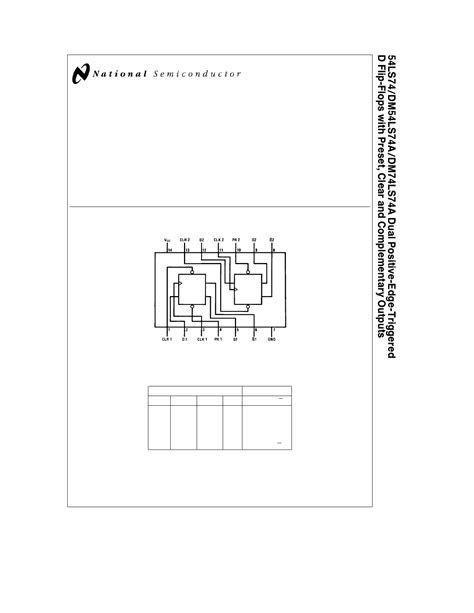
Functional Diagram
The functional diagram of the 74LS74 showcases the internal structure and interconnections of the dual flip-flops:
        +--------------+
  CLR1 -|1           14|- VCC
    D1 -|2           13|- CLR2
  CLK1 -|3           12|- D2
  PRE1 -|4    74LS74 11|- CLK2
    Q1 -|5           10|- PRE2
   Q1_N-|6            9|- Q2
   GND -|7            8|- Q2_N
        +--------------+

How the 74LS74 Dual Flip-flop Works
D Flip-flop Operation
The 74LS74 contains two independent D-type flip-flops. Each flip-flop has a data input (D), a clock input (CLK), a preset input (PRE), a clear input (CLR), and two outputs (Q and Q_N). The flip-flop’s output (Q) follows the state of the data input (D) on the positive edge of the clock signal.
Truth Table
The truth table for each flip-flop in the 74LS74 is as follows:
| PRE | CLR | CLK | D | Q | Q_N |
|---|---|---|---|---|---|
| L | H | X | X | H | L |
| H | L | X | X | L | H |
| L | L | X | X | H* | L* |
| H | H | ↑ | L | L | H |
| H | H | ↑ | H | H | L |
| H | H | L/H | X | Q0 | Q0_N |
Note: L = Low, H = High, X = Don’t Care, ↑ = Positive edge, Q0 = Previous state, * = Unstable state
Asynchronous Preset and Clear
The 74LS74 features asynchronous preset (PRE) and clear (CLR) inputs for each flip-flop. When the preset input is low, the output (Q) is forced high, regardless of the clock and data inputs. Similarly, when the clear input is low, the output (Q) is forced low. These inputs allow for immediate setting or resetting of the flip-flop’s state.

Applications of the 74LS74 Dual Flip-flop
1. Data Storage and Registers
The 74LS74 can be used as a basic storage element in digital circuits. By cascading multiple flip-flops, you can create registers for storing and manipulating multi-bit data.
2. Frequency Division
The 74LS74 can be used as a frequency divider by connecting the inverted output (Q_N) to the data input (D). This configuration divides the input clock frequency by two, producing a signal with half the original frequency.
3. Debouncing Switches
Mechanical switches often produce multiple transitions when pressed or released, causing unwanted signal bounces. The 74LS74 can be used to debounce these switches by sampling the switch state on the clock edge and storing the stable state in the flip-flop.
4. Shift Registers
By connecting multiple 74LS74 flip-flops in series, you can create shift registers for serial-to-parallel or parallel-to-serial data conversion. The data is shifted through the flip-flops on each clock cycle, allowing for data manipulation and storage.
5. Synchronization and Clock Domain Crossing
The 74LS74 can be used to synchronize asynchronous signals or to transfer data between different clock domains. By sampling the asynchronous signal with the flip-flop’s clock, you can ensure stable and synchronized data transfer.

Interfacing the 74LS74 with Other Logic Families
The 74LS74 is part of the 74LS (Low-power Schottky) logic family, which is compatible with other TTL (Transistor-Transistor Logic) families. However, when interfacing with different logic families, such as CMOS, you should consider the following:
-
Voltage Levels: Ensure that the voltage levels of the connected devices are compatible. The 74LS74 operates with a supply voltage of 5V, while CMOS devices may have different voltage requirements.
-
Drive Current: The 74LS74 has a limited drive current capability. If you need to drive high-capacitance loads or multiple devices, consider using buffer ICs or transistors to amplify the output current.
-
Input Thresholds: Different logic families have different input threshold voltages. Make sure that the output levels of the connected devices meet the input requirements of the 74LS74.
Frequently Asked Questions (FAQ)
1. What is the difference between the 74LS74 and the 7474?
The 74LS74 and 7474 are functionally similar, as both are dual D-type flip-flops. However, the 74LS74 is part of the Low-power Schottky (LS) family, which offers improved speed and lower power consumption compared to the original 7474.
2. Can the 74LS74 be used as a T flip-flop?
No, the 74LS74 is a D-type flip-flop and cannot be directly used as a T flip-flop. However, you can create a T flip-flop by connecting the inverted output (Q_N) to the data input (D), which will toggle the output state on each clock pulse.
3. What is the maximum clock frequency for the 74LS74?
The maximum clock frequency for the 74LS74 depends on the specific version and manufacturer. Typically, it can operate at frequencies up to 25 MHz or higher. Consult the device’s datasheet for accurate specifications.
4. How do I connect the unused inputs of the 74LS74?
If you are not using one of the flip-flops in the 74LS74, it is recommended to tie the unused inputs (PRE, CLR, and D) to a stable voltage level (e.g., VCC for PRE and D, GND for CLR) to prevent floating inputs and ensure proper operation of the used flip-flop.
5. Can I use the 74LS74 in a 3.3V system?
The 74LS74 is designed for 5V operation. While it may work in a 3.3V system, it is not guaranteed, and the voltage levels may not be compatible. For 3.3V systems, it is recommended to use flip-flops specifically designed for that voltage level, such as the 74LVC74 or 74HC74.
Conclusion
The 74LS74 dual flip-flop is a versatile and widely used IC in digital electronics. Its ability to store data, synchronize signals, and perform frequency division makes it an essential component in many circuits. By understanding its functionality, pinout, and applications, you can effectively incorporate the 74LS74 into your designs and harness its capabilities. Always refer to the device’s datasheet for specific details and considerations when using the 74LS74 in your projects.


Leave a Reply