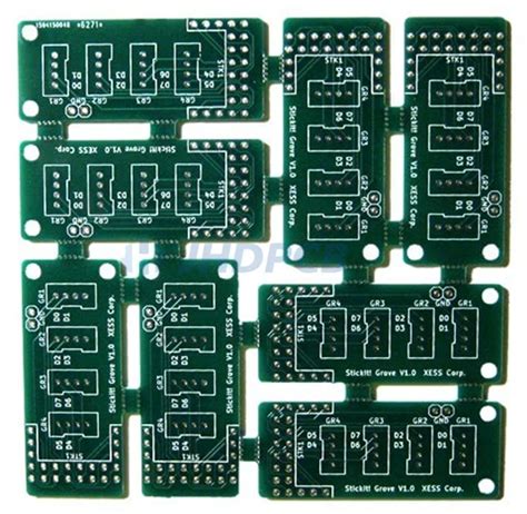
What is PCB Panelization?
PCB panelization is the process of arranging multiple PCB designs on a single panel to optimize the manufacturing process. This technique allows for the simultaneous production of several PCBs, reducing the overall manufacturing time and cost. The panel is designed to accommodate the specific requirements of the PCB manufacturer, such as the panel size, materials, and fabrication techniques.
Benefits of PCB Panelization
- Cost reduction: By producing multiple PCBs on a single panel, the manufacturing cost per unit is significantly reduced.
- Improved efficiency: Panelization streamlines the fabrication process, reducing the time required for setup and handling.
- Increased yield: Proper panelization minimizes the risk of damage during the manufacturing process, resulting in higher yield rates.
PCB Panelization Design Considerations
When designing a PCB panel, several factors must be taken into account to ensure optimal results. These considerations include:
1. Panel Size and Material
The panel size and material are determined by the capabilities of the PCB manufacturer and the specific requirements of the project. Common panel sizes include:
| Panel Size | Dimensions (mm) |
|---|---|
| Small | 200 x 200 |
| Medium | 300 x 300 |
| Large | 400 x 400 |
The most commonly used material for PCB panels is FR-4, a glass-reinforced epoxy laminate. Other materials, such as aluminum or flexible substrates, may be used for specific applications.
2. Spacing and Clearance
Proper spacing and clearance between individual PCBs on the panel are essential to ensure accurate fabrication and prevent damage during the depaneling process. The minimum spacing between boards should be:
| Spacing Type | Minimum Distance (mm) |
|---|---|
| Board to Board | 2.0 |
| Board to Edge | 3.0 |
Additionally, designers should include fiducial marks and tooling holes to aid in the alignment and registration of the panel during the manufacturing process.
3. Panelization Methods
There are several methods for panelizing PCBs, each with its own advantages and limitations. The most common methods include:
- V-Scoring: V-shaped grooves are cut into the panel, allowing for easy separation of the individual PCBs.
- Tab Routing: Small tabs are left connecting the PCBs, which can be easily broken after fabrication.
- Perforated Routing: A series of closely spaced holes are drilled along the edges of the PCBs, allowing for easy separation.
The choice of panelization method depends on the specific requirements of the project, such as the PCB thickness, material, and the desired level of automation in the depaneling process.
4. Copper Balancing
Copper balancing is the process of ensuring an even distribution of copper across the PCB panel. Uneven copper distribution can lead to warping, twisting, or other distortions during the fabrication process. To achieve proper copper balancing, designers should:
- Distribute copper evenly across the panel
- Add copper thieving patterns in areas with low copper density
- Avoid large, solid copper areas
5. Solder Mask and Silkscreen
Solder mask and silkscreen are essential elements of PCB design that protect the copper traces and provide useful information for assembly and debugging. When panelizing PCBs, designers should consider:
- Solder mask expansion: Allow for a minimum of 0.1mm solder mask expansion to ensure proper coverage of the copper traces.
- Silkscreen legibility: Ensure that silkscreen text and symbols are legible and properly aligned on each individual PCB.
6. Assembly Considerations
PCB panelization design should also take into account the requirements of the assembly process. This includes:
- Component placement: Ensure that components are placed at least 2mm away from the edge of the PCB to avoid damage during depaneling.
- Depaneling methods: Consider the depaneling method when designing the panel, as some methods may require additional clearance or special features.
7. Testing and Inspection
Incorporating testing and inspection features into the PCB panelization design can streamline the quality control process. This may include:
- Test coupons: Include test coupons on the panel to verify the quality of the fabrication process.
- Fiducial marks: Add fiducial marks to aid in the alignment and inspection of the PCBs during assembly.

PCB Panelization Best Practices
To ensure the best results when panelizing PCBs, designers should follow these best practices:
- Communicate with the PCB manufacturer early in the design process to understand their specific requirements and capabilities.
- Use a consistent grid size and spacing for all PCBs on the panel to simplify the panelization process.
- Incorporate symmetry in the panel design to minimize warping and ensure even copper distribution.
- Use rounded corners and avoid sharp angles to reduce stress concentrations and improve manufacturability.
- Verify the panel design using design rule checks (DRC) and manufacturing rule checks (MRC) to identify and correct any potential issues.

Frequently Asked Questions (FAQ)
1. What is the minimum spacing between PCBs on a panel?
The minimum spacing between PCBs on a panel should be 2.0mm for board-to-board spacing and 3.0mm for board-to-edge spacing. This ensures accurate fabrication and prevents damage during the depaneling process.
2. What is copper balancing, and why is it important?
Copper balancing is the process of ensuring an even distribution of copper across the PCB panel. It is important because uneven copper distribution can lead to warping, twisting, or other distortions during the fabrication process.
3. What are the most common panelization methods?
The most common panelization methods are V-scoring, tab routing, and perforated routing. The choice of method depends on the specific requirements of the project, such as the PCB thickness, material, and the desired level of automation in the depaneling process.
4. How can I incorporate testing and inspection features into my PCB panelization design?
You can incorporate testing and inspection features into your PCB panelization design by including test coupons on the panel to verify the quality of the fabrication process and adding fiducial marks to aid in the alignment and inspection of the PCBs during assembly.
5. What are some best practices for PCB panelization design?
Some best practices for PCB panelization design include communicating with the PCB manufacturer early in the design process, using a consistent grid size and spacing for all PCBs on the panel, incorporating symmetry in the panel design, using rounded corners and avoiding sharp angles, and verifying the panel design using design rule checks (DRC) and manufacturing rule checks (MRC).

Conclusion
PCB panelization is a critical aspect of PCB design that can significantly impact the manufacturing process’s efficiency, cost, and quality. By understanding the key considerations and best practices for PCB panelization design, designers can create panels that optimize the fabrication process and ensure the highest quality end products. From panel size and material selection to spacing and clearance requirements, copper balancing, and assembly considerations, designers must carefully evaluate each aspect of the panelization process to achieve the best results. By following the guidelines and best practices outlined in this article, designers can unlock the full potential of PCB panelization and create designs that are both efficient and reliable.


Leave a Reply