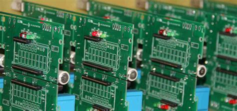
1. Component Selection and Placement
The first point to consider in PCB Assembly is the selection and placement of electronic components. It is essential to choose components that meet the design specifications, are compatible with each other, and are readily available. The placement of the components on the PCB should be optimized for functionality, manufacturability, and testability.
1.1 Component Selection Criteria
When selecting components for PCB assembly, consider the following criteria:
- Functionality: Choose components that meet the required electrical and performance specifications.
- Compatibility: Ensure that the selected components are compatible with each other and the PCB materials.
- Availability: Select components that are readily available and have a reliable supply chain to avoid delays in production.
- Cost: Consider the cost of the components and their impact on the overall production budget.
1.2 Component Placement Guidelines
Follow these guidelines when placing components on the PCB:
- Functionality: Group related components together and place them close to their associated circuitry to minimize signal integrity issues.
- Manufacturability: Ensure that the component placement allows for efficient assembly processes, such as automated pick-and-place and soldering.
- Testability: Place test points and connectors in easily accessible locations to facilitate testing and debugging.
- Thermal management: Consider the heat dissipation requirements of the components and place them accordingly to avoid thermal issues.
2. Solder Paste Application
The second point to consider in PCB assembly is the application of solder paste. Solder paste is a mixture of tiny solder particles and flux that is applied to the PCB pads before component placement. The quality and consistency of the solder paste application directly affect the soldering process and the final assembly quality.
2.1 Solder Paste Properties
When selecting solder paste for PCB assembly, consider the following properties:
- Alloy composition: Choose a solder paste with an alloy composition that matches the requirements of the components and the PCB materials.
- Particle size: Select a solder paste with the appropriate particle size for the pad dimensions and the desired solder joint profile.
- Flux activity: Choose a solder paste with the appropriate flux activity level based on the surface finishes of the components and the PCB.
- Viscosity: Select a solder paste with the appropriate viscosity for the chosen application method (e.g., stencil printing, dispensing).
2.2 Solder Paste Application Methods
There are two common methods for applying solder paste to PCBs:
- Stencil Printing:
- A stencil with apertures corresponding to the PCB pads is placed over the PCB.
- Solder paste is applied onto the stencil and spread across the surface using a squeegee.
-
The stencil is then removed, leaving solder paste deposits on the PCB pads.
-
Dispensing:
- Solder paste is dispensed directly onto the PCB pads using a dispensing machine or syringe.
- This method is suitable for low-volume production or when precise control over the solder paste volume is required.
| Method | Advantages | Disadvantages |
|---|---|---|
| Stencil Printing | – High-speed process | – Requires stencil fabrication |
| – Suitable for high-volume production | – Limited flexibility for design changes | |
| – Consistent solder paste deposits | – Stencil cleaning and maintenance required | |
| Dispensing | – Flexible and adaptable to design changes | – Slower process compared to stencil printing |
| – Precise control over solder paste volume | – Higher equipment and material costs | |
| – Suitable for low-volume or prototype builds | – Requires frequent calibration and setup |

3. Reflow Soldering
The third point to consider in PCB assembly is the reflow soldering process. Reflow soldering is a process where the PCB with the placed components and solder paste is heated in a controlled manner to melt the solder and form permanent connections between the components and the PCB pads.
3.1 Reflow Soldering Profile
A reflow soldering profile defines the temperature and time parameters for the reflow process. A typical reflow profile consists of four stages:
- Preheat: The PCB is gradually heated to activate the flux and evaporate the solvents in the solder paste.
- Soak: The PCB is held at a constant temperature to ensure even heating and to allow the components to reach thermal equilibrium.
- Reflow: The temperature is rapidly increased to melt the solder particles and form solder joints between the components and the PCB pads.
- Cooling: The PCB is cooled down gradually to solidify the solder joints and prevent thermal shock to the components.
3.2 Reflow Soldering Equipment
There are two main types of reflow soldering equipment:
- Convection Reflow Oven:
- Uses forced convection heating to heat the PCB and components.
- Provides even heating and good temperature control.
-
Suitable for high-volume production and large PCBs.
-
Infrared (IR) Reflow Oven:
- Uses infrared radiation to heat the PCB and components.
- Provides faster heating compared to convection ovens.
- Suitable for smaller PCBs and low-volume production.
| Equipment Type | Advantages | Disadvantages |
|---|---|---|
| Convection Reflow Oven | – Even heating and good temperature control | – Slower heating compared to IR ovens |
| – Suitable for large PCBs and high-volume | – Higher energy consumption | |
| – Reduced risk of component damage | – Larger footprint and higher capital cost | |
| Infrared (IR) Reflow Oven | – Faster heating compared to convection | – Uneven heating and potential hot spots |
| – Suitable for smaller PCBs and low-volume | – Risk of component damage due to rapid heating | |
| – Compact size and lower capital cost | – Limited control over temperature profiles |

4. Inspection and Testing
The fourth point to consider in PCB assembly is inspection and testing. Inspection and testing are critical steps to ensure the quality and functionality of the assembled PCBs. There are various methods and techniques used for inspection and testing, depending on the complexity of the PCB and the required level of assurance.
4.1 Visual Inspection
Visual inspection is the first step in the inspection process and involves examining the assembled PCB for any visible defects or anomalies. Common visual inspection techniques include:
- Manual inspection using magnifying lenses or microscopes
- Automated optical inspection (AOI) using machine vision systems
Visual inspection helps identify issues such as:
- Misaligned or missing components
- Solder bridges or insufficient solder joints
- Damaged or lifted components
- Contamination or foreign objects on the PCB
4.2 Electrical Testing
Electrical testing involves verifying the electrical functionality and performance of the assembled PCB. Common electrical testing methods include:
- In-circuit testing (ICT): Probes are used to test individual components and their connections on the PCB.
- Functional testing: The PCB is powered up and tested for its intended functionality using test fixtures or automated test equipment (ATE).
- Boundary scan testing: Uses built-in test circuitry (JTAG) to test the interconnections and functionality of the components on the PCB.
Electrical testing helps identify issues such as:
- Open or short circuits
- Incorrect component values or polarities
- Faulty or non-functional components
- Signal integrity or timing issues

5. Rework and Repair
The fifth point to consider in PCB assembly is rework and repair. Despite best efforts, there may be instances where assembled PCBs require rework or repair due to manufacturing defects or component failures. Rework and repair processes aim to correct these issues while minimizing damage to the PCB and surrounding components.
5.1 Rework Processes
Rework processes involve the removal and replacement of defective components or the correction of soldering issues. Common rework techniques include:
- Desoldering: Removing the defective component using desoldering tools such as desoldering irons, desoldering stations, or hot air rework stations.
- Resoldering: Applying new solder and soldering the replacement component onto the PCB.
- Solder joint repair: Correcting insufficient or bridged solder joints using soldering irons or solder rework stations.
5.2 Repair Processes
Repair processes involve the correction of PCB defects or damage without replacing components. Common repair techniques include:
- Trace repair: Repairing damaged or broken PCB traces using conductive epoxy, jumper wires, or micro-soldering techniques.
- Pad repair: Repairing damaged or lifted PCB pads using conductive epoxy or specialized repair pads.
- Conformal coating repair: Repairing damaged or removed conformal coating using specialized coating materials and application techniques.
6. Documentation and Traceability
The sixth and final point to consider in PCB assembly is documentation and traceability. Proper documentation and traceability are essential for maintaining quality control, troubleshooting, and ensuring compliance with regulations and standards.
6.1 Documentation
Proper documentation in PCB assembly includes:
- Bill of Materials (BOM): A comprehensive list of all components used in the PCB assembly, including part numbers, quantities, and specifications.
- Assembly drawings: Detailed drawings showing the component placement, orientation, and soldering requirements for the PCB assembly.
- Work instructions: Step-by-step instructions for the assembly process, including any special handling or processing requirements.
- Inspection and test procedures: Documented procedures for visual inspection, electrical testing, and quality control checks.
6.2 Traceability
Traceability in PCB assembly involves the ability to track and trace the materials, components, and processes used in the production of each individual PCB. Traceability is important for:
- Quality control: Identifying and isolating defective components or processes in case of quality issues or failures.
- Regulatory compliance: Meeting traceability requirements for industries such as aerospace, medical, or automotive.
- Material management: Tracking the usage and inventory of components and materials used in the PCB assembly.
Traceability can be achieved through the use of:
- Unique identifiers: Assigning unique serial numbers or barcodes to each PCB and tracking them throughout the assembly process.
- Lot tracking: Tracking the lot numbers of components and materials used in each PCB assembly.
- Date codes: Recording the date codes of components and materials used in the assembly process.
- Traceability software: Using specialized software solutions to manage and track the traceability data throughout the production process.
Frequently Asked Questions (FAQ)
- What is the difference between through-hole and surface-mount PCB assembly?
-
Through-hole assembly involves inserting component leads through holes drilled in the PCB and soldering them on the opposite side. Surface-mount assembly involves placing components directly onto the surface of the PCB and soldering them in place. Surface-mount assembly allows for smaller components and higher component density compared to through-hole assembly.
-
What are some common defects that can occur in PCB assembly?
-
Some common defects in PCB assembly include:
- Solder bridges: Unintended connections between adjacent solder joints.
- Cold solder joints: Weak or incomplete solder joints due to insufficient heat or poor wetting.
- Tombstoning: Components standing up on one end due to uneven heating or solder paste application.
- Component shifting: Components moving out of their intended position during the reflow process.
-
How can I ensure the reliability and longevity of my PCB assembly?
-
To ensure the reliability and longevity of your PCB assembly:
- Use high-quality components from reputable suppliers.
- Follow best practices for component placement, solder paste application, and reflow soldering.
- Perform thorough inspection and testing to identify and correct any defects or issues.
- Use appropriate protection methods such as conformal coating or potting for harsh environments.
-
What are some considerations for PCB assembly in high-mix low-volume production?
-
For high-mix low-volume PCB assembly:
- Use flexible and modular assembly processes that can accommodate frequent changeovers.
- Implement lean manufacturing principles to minimize waste and optimize inventory management.
- Use automated equipment with quick changeover capabilities to reduce setup times.
- Maintain good documentation and traceability to ensure quality control and efficient troubleshooting.
-
How can I choose the right PCB assembly partner for my project?
- When choosing a PCB assembly partner, consider the following factors:
- Technical capabilities and experience in your specific industry or application.
- Quality management systems and certifications (e.g., ISO 9001, IPC standards).
- Production capacity and lead times that match your project requirements.
- Communication and customer support to ensure smooth collaboration and issue resolution.
- Cost competitiveness and value-added services that align with your project budget and goals.
By paying attention to these six essential points in PCB assembly – component selection and placement, solder paste application, reflow soldering, inspection and testing, rework and repair, and documentation and traceability – you can ensure a high-quality and reliable PCB assembly process for your electronics manufacturing projects.


Leave a Reply