PCB Essentials: Understanding the Basics of 4 Layer PCBs
Introduction to 4 Layer PCBs
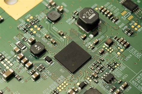
A 4 layer PCB, or printed circuit board, is a complex electronic component that consists of four conductive layers laminated together with insulating material. These boards are widely used in various applications, from consumer electronics to industrial equipment, due to their ability to accommodate high component density and improved signal integrity compared to simpler 2 layer PCBs.
Advantages of Using 4 Layer PCBs
- Increased routing space
- Better signal integrity
- Reduced electromagnetic interference (EMI)
- Improved power distribution
- Enhanced mechanical stability
4 Layer PCB Stackup
A typical 4 layer PCB stackup consists of the following layers:
| Layer | Description |
|---|---|
| Top Layer | Signal layer, components, and routing |
| Ground Plane | Provides a reference ground and reduces EMI |
| Power Plane | Distributes power to components |
| Bottom Layer | Signal layer, components, and routing |
Signal Layers
The top and bottom layers of a 4 layer PCB are primarily used for component placement and signal routing. These layers are where the majority of the components are soldered, and the traces connecting them are routed.
Ground and Power Planes
The inner layers of a 4 layer PCB are dedicated to ground and power planes. The ground plane provides a low-impedance reference point for the signals on the outer layers, reducing EMI and improving signal integrity. The power plane distributes power evenly across the board, ensuring stable voltage delivery to all components.
Designing 4 Layer PCBs
Design Considerations
When designing a 4 layer PCB, several factors must be considered to ensure optimal performance and manufacturability:
- Component placement
- Signal routing
- Via placement and drilling
- Layer stackup and spacing
- Impedance control
PCB Design Software
To design a 4 layer PCB, you’ll need to use specialized PCB design software. Some popular options include:
- Altium Designer
- KiCad
- Eagle
- OrCAD
These software packages allow you to create schematic diagrams, design the PCB layout, and generate manufacturing files.
Manufacturing 4 Layer PCBs
PCB Fabrication Process
The manufacturing process for 4 layer PCBs involves several steps:
- Creating the copper layers
- Laminating the layers together
- Drilling via holes
- Plating the via holes and outer layers
- Applying solder mask and silkscreen
- Surface finishing (e.g., HASL, ENIG, or OSP)
Choosing a PCB Manufacturer
When selecting a PCB manufacturer, consider the following factors:
- Experience with 4 layer PCBs
- Manufacturing capabilities and quality control
- Lead times and pricing
- Customer support and communication
Testing and Validation
Electrical Testing
Before assembling components on a 4 layer PCB, it’s essential to perform electrical testing to ensure the board’s integrity. Common tests include:
- Continuity testing
- Insulation resistance testing
- High-potential (HiPot) testing
Functional Testing
After assembling the components, functional testing is performed to verify that the board operates as intended. This may involve:
- Power-on testing
- Signal integrity testing
- Boundary scan testing
- In-circuit testing
Applications of 4 Layer PCBs
4 layer PCBs are used in a wide range of applications, including:
- Consumer electronics (smartphones, tablets, laptops)
- Automotive electronics (infotainment systems, engine control units)
- Medical devices (patient monitors, imaging equipment)
- Industrial automation (PLCs, sensors, control systems)
- Telecommunications (routers, switches, base stations)
Troubleshooting and Repair
Common Issues with 4 Layer PCBs
Despite careful design and manufacturing, issues can still arise with 4 layer PCBs. Some common problems include:
- Open or short circuits
- Incorrect component placement
- Solder joint defects
- Signal integrity issues
- Thermal management problems
Debugging Techniques
When troubleshooting a 4 layer PCB, several techniques can be used to identify and resolve issues:
- Visual inspection
- Continuity testing
- Thermal imaging
- Signal analysis using oscilloscopes or logic analyzers
- In-circuit emulation and debugging
Rework and Repair
If a problem is identified, the board may need to be reworked or repaired. This can involve:
- Desoldering and replacing components
- Repairing or adding traces and vias
- Applying conformal coating or other protective measures
Future Trends in 4 Layer PCB Technology
As electronic devices continue to advance, 4 layer PCB technology is evolving to meet new challenges and requirements. Some emerging trends include:
- High-density interconnect (HDI) designs
- Embedded components
- Flexible and rigid-flex PCBs
- Advanced materials (e.g., low-loss dielectrics, high-temperature substrates)
- 3D printing of PCBs
Frequently Asked Questions (FAQ)
-
What is the difference between a 2 layer and 4 layer PCB?
A 2 layer PCB has only two conductive layers (top and bottom), while a 4 layer PCB has four conductive layers (top, ground plane, power plane, and bottom). 4 layer PCBs offer more routing space, better signal integrity, and reduced EMI compared to 2 layer PCBs. -
When should I use a 4 layer PCB instead of a 2 layer PCB?
You should consider using a 4 layer PCB when your design requires high component density, improved signal integrity, or reduced EMI. 4 layer PCBs are also a good choice for designs with complex power distribution requirements or high-speed signals. -
How much does a 4 layer PCB cost compared to a 2 layer PCB?
4 layer PCBs are generally more expensive than 2 layer PCBs due to the additional materials and manufacturing steps involved. The exact cost difference depends on factors such as board size, quantity, and manufacturing location, but you can expect to pay 50-100% more for a 4 layer PCB compared to a similar 2 layer design. -
Can I design a 4 layer PCB using the same software as a 2 layer PCB?
Yes, most PCB design software packages support the creation of 4 layer PCBs. However, designing a 4 layer PCB requires additional considerations, such as layer stackup, via placement, and impedance control, which may require more advanced features or knowledge. -
How long does it take to manufacture a 4 layer PCB?
The manufacturing time for a 4 layer PCB depends on the complexity of the design, the chosen manufacturer, and the desired quantity. Typical lead times range from 1-3 weeks, but expedited services may be available for an additional cost. It’s important to communicate your timeline requirements clearly with your chosen PCB manufacturer.
Conclusion
4 layer PCBs are a critical component in modern electronic devices, offering increased routing space, improved signal integrity, and reduced EMI compared to simpler 2 layer designs. By understanding the basics of 4 layer PCB design, manufacturing, and testing, you can create more advanced and reliable electronic products. As technology continues to evolve, staying up-to-date with the latest trends and techniques in 4 layer PCB development will be essential for success in the competitive electronics industry.


Leave a Reply