1. Visual Inspection
The first and most basic method of checking for soldering defects is visual inspection. This process involves carefully examining the soldered joints and components on the PCB Board using the naked eye or a magnifying glass. Some common defects that can be detected through visual inspection include:
- Bridging: When solder accidentally connects two or more pins or pads that should not be connected.
- Insufficient solder: When there is not enough solder to create a proper joint, resulting in a weak or unreliable connection.
- Excess solder: When there is too much solder on a joint, which can cause short circuits or impede the proper functioning of the component.
- Cold joints: When the solder does not flow properly, resulting in a dull, grainy, or cracked appearance.
To perform a visual inspection effectively, ensure that you have adequate lighting and a clear view of the PCB board. Use a magnifying glass or microscope for smaller components and joints.
2. X-Ray Inspection
X-ray inspection is a non-destructive testing method that uses X-rays to create images of the internal structure of the soldered joints. This method is particularly useful for detecting defects that are not visible to the naked eye, such as:
- Voids: Small air bubbles trapped within the solder joint, which can weaken the connection and lead to failures.
- Insufficient penetration: When the solder does not flow through the entire joint, resulting in a weak or incomplete connection.
- Barrel fill: The amount of solder present inside a through-hole component’s barrel, which is crucial for ensuring a reliable connection.
X-ray inspection systems come in various types, including 2D and 3D systems, each with its own advantages and limitations. 2D systems are more affordable and faster but may not provide as much detail as 3D systems, which offer a more comprehensive view of the solder joint’s internal structure.

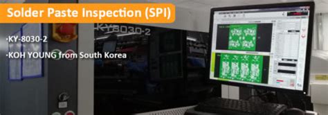
3. Automated Optical Inspection (AOI)
Automated Optical Inspection (AOI) is a computer-based system that uses high-resolution cameras and advanced image processing algorithms to detect soldering defects on PCB boards. AOI systems can identify a wide range of defects, including:
- Component placement errors
- Solder bridging
- Insufficient or excess solder
- Lifted leads
- Tombstoning (when a component stands up on one end due to uneven heating)
AOI systems are highly efficient and can inspect a large number of PCB boards quickly and accurately. They also provide consistent results, eliminating the subjectivity associated with manual visual inspection.

4. In-Circuit Testing (ICT)
In-Circuit Testing (ICT) is a method that uses specialized equipment to test the functionality of individual components on a PCB board. ICT systems use a bed-of-nails fixture that makes contact with specific test points on the PCB, allowing the system to measure the electrical properties of each component and detect any defects or malfunctions.
ICT can detect various defects, including:
- Incorrect component values
- Shorted or open circuits
- Backward or missing components
- Defective or damaged components
ICT is an effective method for detecting functional defects that may not be visually apparent, ensuring that the PCB board functions as intended.

5. Flying Probe Testing
Flying Probe Testing is another automated method for testing the functionality of PCB boards. Unlike ICT, which uses a fixed bed-of-nails fixture, Flying Probe Testing employs movable test probes that can access any point on the PCB board. This flexibility makes Flying Probe Testing ideal for testing small batches or prototypes, as it eliminates the need for custom test fixtures.
Flying Probe Testing can detect a wide range of defects, including:
- Shorts and opens
- Incorrect component values
- Missing or misplaced components
- Defective or damaged components
Flying Probe Testing is generally slower than ICT but offers greater flexibility and adaptability, making it a valuable tool for PCB inspection.
6. Boundary Scan Testing
Boundary Scan Testing, also known as JTAG (Joint Test Action Group) testing, is a method that uses a special test access port (TAP) built into the integrated circuits (ICs) on a PCB board. This TAP allows the testing system to access and control the individual pins of the ICs, enabling it to test for defects and malfunctions.
Boundary Scan Testing can detect various defects, including:
- Shorts and opens
- Stuck-at faults (when a pin is stuck at a logical high or low state)
- Component interconnection faults
- Programming errors in programmable devices
Boundary Scan Testing is particularly useful for testing complex, high-density PCB boards with limited physical access to test points.
7. Functional Testing
Functional Testing is a method that tests the overall functionality of a PCB board by simulating its intended operating conditions. This type of testing ensures that the PCB board performs as expected when subjected to real-world scenarios.
Functional Testing can detect defects such as:
- Incorrect component operation
- Signal integrity issues
- Timing errors
- Compatibility problems between components
Functional Testing is typically performed after the PCB board has passed other inspection methods, as it confirms that the board functions correctly as a whole.
8. Burn-In Testing
Burn-In Testing is a method that subjects the PCB board to elevated temperatures and voltages for an extended period to identify any defects or weaknesses that may not be apparent under normal operating conditions. This type of testing accelerates the aging process, allowing defects to manifest themselves more quickly.
Burn-In Testing can detect defects such as:
- Early-life failures (infant mortality)
- Temperature-dependent defects
- Intermittent faults
- Component degradation
Burn-In Testing is particularly useful for PCB boards that will be used in harsh environments or critical applications where reliability is paramount.
9. Microsectioning
Microsectioning is a destructive testing method that involves cutting a cross-section of a soldered joint and examining it under a microscope. This method provides a detailed view of the internal structure of the joint, allowing for the detection of defects that may not be visible through other inspection methods.
Microsectioning can detect defects such as:
- Voids
- Cracks
- Intermetallic formation
- Insufficient or excessive solder penetration
While microsectioning is a valuable tool for analyzing soldering defects, it is a destructive process and should be used sparingly, typically for failure analysis or process optimization.
10. Electrical Testing
Electrical Testing is a method that involves measuring the electrical characteristics of the PCB board and its components to ensure that they meet the specified requirements. This type of testing can be performed at various stages of the PCB assembly process, including bare board testing, in-circuit testing, and functional testing.
Electrical Testing can detect defects such as:
- Short circuits
- Open circuits
- Incorrect component values
- Signal integrity issues
- Power supply problems
Electrical Testing is essential for ensuring that the PCB board functions correctly and meets the required specifications.
Frequently Asked Questions (FAQ)
- What is the most common soldering defect on PCB boards?
-
The most common soldering defect on PCB boards is solder bridging, which occurs when solder accidentally connects two or more pins or pads that should not be connected.
-
Can all soldering defects be detected visually?
-
No, not all soldering defects can be detected visually. Some defects, such as voids or insufficient solder penetration, may require X-ray inspection or other advanced testing methods to identify.
-
Is Automated Optical Inspection (AOI) better than manual visual inspection?
-
AOI is generally more efficient and accurate than manual visual inspection, as it can inspect a large number of PCB boards quickly and consistently, eliminating the subjectivity associated with human inspection.
-
What is the difference between In-Circuit Testing (ICT) and Flying Probe Testing?
-
ICT uses a fixed bed-of-nails fixture to make contact with specific test points on the PCB board, while Flying Probe Testing employs movable test probes that can access any point on the board. Flying Probe Testing offers greater flexibility and adaptability but is generally slower than ICT.
-
Is Burn-In Testing necessary for all PCB boards?
- Burn-In Testing is particularly useful for PCB boards that will be used in harsh environments or critical applications where reliability is paramount. However, not all PCB boards require Burn-In Testing, and the decision to perform this type of testing should be based on the specific requirements and intended use of the board.
Conclusion
Checking for defects on soldering PCB boards is a critical process that ensures the proper functioning and reliability of electronic devices. By employing a combination of visual inspection, advanced testing methods, and automated systems, manufacturers can identify and address a wide range of soldering defects, from simple bridging to complex functional issues.
Implementing a comprehensive PCB inspection strategy that incorporates the 10 helpful methods discussed in this article can help improve the quality, reliability, and performance of electronic devices, ultimately leading to higher customer satisfaction and reduced costs associated with defects and failures.


Leave a Reply