Introduction to 8-Layer PCBs
An 8-layer PCB (Printed Circuit Board) is a complex, high-density circuit board that consists of eight conductive copper layers laminated together with insulating material. These advanced PCBs are designed to accommodate a large number of components and interconnections, making them ideal for applications that require high performance, reliability, and miniaturization.
Benefits of 8-Layer PCBs
-
Increased Density: 8-layer PCBs allow for a higher component density compared to boards with fewer layers. This enables the design of more compact and space-efficient electronic devices.
-
Improved Signal Integrity: The additional layers in an 8-layer PCB provide better signal routing options, reducing crosstalk and electromagnetic interference (EMI). This results in cleaner and more stable signals.
-
Enhanced Power Distribution: With more layers available, power and ground planes can be strategically placed to minimize noise and ensure efficient power distribution throughout the board.
-
Faster Signal Transmission: The increased number of layers allows for shorter signal paths, which reduces signal propagation delays and enables faster operating speeds.
Applications of 8-Layer PCBs
8-layer PCBs find applications in various industries and products, including:
- High-performance computing systems
- Telecommunications equipment
- Medical devices
- Aerospace and defense systems
- Automotive electronics
- Industrial control systems
Advantages of 8-Layer PCBs over Fewer Layer Boards
Comparison of Layer Count and Board Complexity
| Layer Count | Complexity | Typical Applications |
|---|---|---|
| 1-2 | Low | Simple circuits, hobbyist projects |
| 4 | Medium | Consumer electronics, general-purpose devices |
| 6 | High | Complex digital systems, high-speed devices |
| 8 | Very High | Advanced electronics, high-performance systems |
Space Savings and Miniaturization
One of the primary advantages of using an 8-layer PCB is the ability to create more compact and miniaturized electronic devices. By distributing components and routing across eight layers, designers can significantly reduce the overall footprint of the PCB without compromising functionality.
Example: Smartphone PCBs
Modern smartphones are a prime example of how 8-layer PCBs enable miniaturization. The complex circuitry required for features like high-resolution displays, multi-core processors, and 5G connectivity can be accommodated within the compact form factor of a smartphone thanks to the use of 8-layer PCBs.
Improved Thermal Management
8-layer PCBs offer better thermal management compared to boards with fewer layers. The additional copper layers can be used to create dedicated thermal planes that help dissipate heat generated by components more efficiently. This is particularly important in high-power applications where effective heat dissipation is crucial for ensuring reliable operation and preventing component failure.

Signal Integrity and EMI Reduction
Importance of Signal Integrity
Signal integrity is a critical factor in the performance and reliability of electronic systems. It refers to the quality of electrical signals transmitted through a PCB, ensuring that they maintain their intended characteristics without distortion, attenuation, or interference.
Role of 8-Layer PCBs in Maintaining Signal Integrity
8-layer PCBs play a significant role in maintaining signal integrity by providing advanced routing capabilities and shielding techniques. Some key aspects include:
-
Controlled Impedance: The additional layers in an 8-layer PCB allow for better control over the impedance of signal traces. By carefully designing the trace geometry and dielectric thickness, designers can achieve the desired characteristic impedance, minimizing signal reflections and distortions.
-
Shielding and Isolation: 8-layer PCBs enable the use of dedicated shielding layers, such as ground planes or power planes, to isolate sensitive signals from noise and interference. These layers act as barriers, preventing unwanted electromagnetic coupling between adjacent signal traces.
-
Reduced Crosstalk: The increased number of layers in an 8-layer PCB allows for greater separation between signal traces, reducing the likelihood of crosstalk. By strategically routing signals on different layers and using techniques like guard traces or ground planes, designers can minimize the interaction between signals and maintain signal integrity.
EMI Reduction Techniques in 8-Layer PCBs
Electromagnetic Interference (EMI) is a common problem in electronic systems, where unwanted electromagnetic energy can disrupt the proper functioning of circuits. 8-layer PCBs offer several techniques to reduce EMI:
-
Power and Ground Planes: Dedicating entire layers to power and ground planes helps to create a low-impedance path for return currents. This minimizes the formation of ground loops and reduces the radiation of electromagnetic energy.
-
Shielding Layers: Including shielding layers, such as copper planes or conductive coatings, can effectively contain electromagnetic radiation within the PCB, preventing it from interfering with other devices.
-
Proper Grounding and Routing: Designing a robust grounding scheme and following best practices for signal routing, such as avoiding sharp bends and minimizing loop areas, can significantly reduce EMI in 8-layer PCBs.

High-Speed Design Considerations
Challenges in High-Speed PCB Design
Designing high-speed PCBs presents unique challenges due to the increased frequency and faster edge rates of signals. Some of the key challenges include:
-
Signal Integrity: As signal speeds increase, the impact of factors like impedance mismatch, reflections, and crosstalk becomes more pronounced, requiring careful design considerations to maintain signal integrity.
-
Timing and Synchronization: Ensuring proper timing and synchronization of high-speed signals across the PCB is crucial to avoid data corruption and ensure reliable operation.
-
Power Integrity: High-speed circuits often have stringent power requirements, necessitating the use of advanced power distribution networks and decoupling techniques to minimize voltage fluctuations and maintain stable power delivery.
Advantages of 8-Layer PCBs for High-Speed Design
8-layer PCBs offer several advantages for high-speed design:
-
Controlled Impedance: The additional layers in an 8-layer PCB provide more flexibility in designing controlled impedance traces. By carefully selecting the dielectric material and adjusting the trace geometry, designers can achieve the desired characteristic impedance, minimizing signal reflections and ensuring proper signal propagation.
-
Shortened Signal Paths: With eight layers available, designers can optimize the placement of components and route signals more directly, reducing the overall signal path length. Shorter signal paths minimize propagation delays and help maintain signal integrity at high frequencies.
-
Power and Ground Planes: Dedicated power and ground planes in an 8-layer PCB provide a low-impedance path for power distribution and return currents. This helps to minimize voltage drops, reduce noise, and maintain stable power delivery to high-speed components.
-
Shielding and Isolation: The additional layers in an 8-layer PCB allow for the implementation of shielding techniques, such as the use of ground planes or guard traces, to isolate sensitive high-speed signals from interference and crosstalk.

Cost Considerations and Manufacturing Process
Cost Comparison of Different Layer PCBs
The cost of PCBs generally increases with the number of layers. However, the cost difference between different layer counts can vary depending on factors such as the PCB manufacturer, the volume of the order, and the specific manufacturing requirements.
| Layer Count | Relative Cost |
|---|---|
| 1-2 | Low |
| 4 | Medium |
| 6 | High |
| 8 | Very High |
While 8-layer PCBs are more expensive compared to boards with fewer layers, the cost premium is often justified by the benefits they offer, such as improved performance, reliability, and miniaturization.
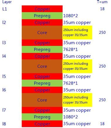
Manufacturing Process for 8-Layer PCBs
The manufacturing process for 8-layer PCBs is more complex compared to boards with fewer layers. It involves the following key steps:
-
Layer Stackup Design: The layer stackup, which defines the arrangement of copper layers and dielectric materials, is carefully designed to meet the electrical and mechanical requirements of the PCB.
-
Lamination: The individual layers of the PCB are laminated together under high pressure and temperature to form a solid board.
-
Drilling: Holes are drilled through the PCB to accommodate component leads and provide electrical connections between layers.
-
Plating: The drilled holes are plated with copper to create conductive pathways between layers.
-
Patterning: The copper layers are selectively etched to create the desired circuit patterns on each layer.
-
Solder Mask and Silkscreen: A solder mask is applied to protect the copper traces, and a silkscreen layer is added for component labeling and identification.
-
Surface Finish: A surface finish, such as HASL (Hot Air Solder Leveling) or ENIG (Electroless Nickel Immersion Gold), is applied to the exposed copper areas to prevent oxidation and enhance solderability.
Conclusion
8-layer PCBs offer numerous benefits for complex and high-performance electronic systems. Their increased density, improved signal integrity, enhanced power distribution, and faster signal transmission make them an ideal choice for applications that demand reliability, miniaturization, and high-speed operation.
While the cost of 8-layer PCBs is higher compared to boards with fewer layers, the advantages they provide often outweigh the additional expense. By leveraging the capabilities of 8-layer PCBs, designers can create advanced electronic devices that meet the ever-increasing demands of modern technology.
Frequently Asked Questions (FAQ)
-
Q: When should I consider using an 8-layer PCB?
A: You should consider using an 8-layer PCB when your design requires high component density, improved signal integrity, enhanced power distribution, or faster signal transmission. 8-layer PCBs are particularly suitable for complex, high-performance applications such as telecommunications equipment, medical devices, and aerospace systems. -
Q: Can 8-layer PCBs be used for high-speed digital designs?
A: Yes, 8-layer PCBs are well-suited for high-speed digital designs. The additional layers provide better control over impedance, allow for shorter signal paths, and enable effective shielding and isolation techniques. These features help maintain signal integrity and minimize issues like crosstalk and EMI in high-speed circuits. -
Q: Are 8-layer PCBs more expensive than boards with fewer layers?
A: Yes, 8-layer PCBs are generally more expensive than boards with fewer layers due to the increased complexity of the manufacturing process and the higher material costs. However, the cost premium is often justified by the benefits they offer, such as improved performance, reliability, and miniaturization. -
Q: How does the manufacturing process differ for 8-layer PCBs compared to boards with fewer layers?
A: The manufacturing process for 8-layer PCBs is more complex and involves additional steps compared to boards with fewer layers. It includes careful layer stackup design, lamination of multiple layers, drilling, plating, patterning, and the application of solder mask and surface finish. The increased complexity requires precise control and specialized equipment to ensure the quality and reliability of the final product. -
Q: Are there any limitations or challenges in designing with 8-layer PCBs?
A: Designing with 8-layer PCBs can present some challenges, particularly in high-speed applications. Signal integrity, timing, and power integrity considerations become more critical, requiring careful design practices and simulation techniques. Additionally, the increased complexity of 8-layer PCBs can make troubleshooting and debugging more challenging compared to simpler designs. However, with proper planning, design tools, and expertise, these challenges can be effectively addressed to harness the full potential of 8-layer PCBs.


Leave a Reply