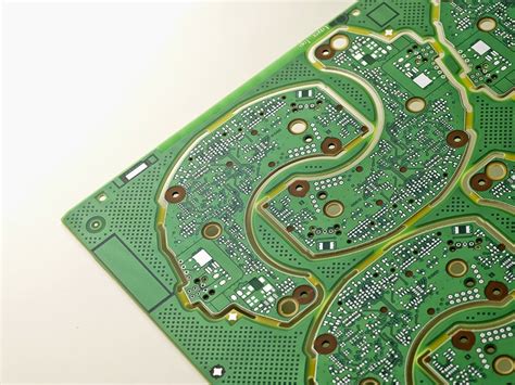
What is an HDI PCB?
HDI PCBs are a type of printed circuit board that features higher wiring density than traditional PCBs. This is achieved through the use of smaller vias, finer trace widths, and tighter spacing between components. HDI PCBs can have multiple layers, with the most common configurations being 4, 6, 8, and 10 layers.
The main characteristics of HDI PCBs include:
- Microvia technology: HDI PCBs use microvias, which are small holes drilled through one or more layers of the PCB to connect different layers. Microvias have a diameter of 0.15mm or less, allowing for higher density connections.
- Fine line width and spacing: HDI PCBs have trace widths and spacing that are typically less than 100 microns (0.1mm), enabling the placement of more components in a smaller area.
- Blind and buried vias: These types of vias are used to connect inner layers of the PCB without being visible on the surface, further increasing the available space for components.
Advantages of HDI PCBs
HDI PCBs offer several advantages over traditional PCBs, making them a preferred choice for many applications:
-
Miniaturization: The higher wiring density of HDI PCBs allows for smaller form factors, enabling the creation of more compact electronic devices.
-
Improved signal integrity: The shorter traces and reduced layer count in HDI PCBs result in improved signal integrity, as there is less opportunity for signal degradation and interference.
-
Increased functionality: With the ability to accommodate more components in a smaller area, HDI PCBs enable the creation of more complex and feature-rich electronic devices.
-
Reduced weight: The compact nature of HDI PCBs leads to a reduction in the overall weight of the electronic device, which is particularly important for portable and aerospace applications.
-
Cost-effective: Although the initial design and fabrication costs of HDI PCBs may be higher than traditional PCBs, they often result in cost savings in the long run due to reduced assembly time and improved reliability.

Applications of HDI PCBs
HDI PCBs find applications in various industries and products, such as:
- Smartphones and tablets
- Wearable electronics
- Medical devices
- Aerospace and defense systems
- Automotive electronics
- Industrial automation and control systems
- High-performance computing

HDI PCB Design Considerations
When designing an HDI PCB, there are several factors to consider to ensure optimal performance and manufacturability:
-
Layer stack-up: Determine the appropriate number of layers and their arrangement based on the complexity of the circuit and the required signal integrity.
-
Via types and placement: Select the appropriate via types (microvia, blind, or buried) and optimize their placement to minimize signal path length and improve routing efficiency.
-
Trace width and spacing: Adhere to the minimum trace width and spacing guidelines for the chosen HDI PCB technology to ensure proper manufacturability and signal integrity.
-
Component placement: Optimize component placement to minimize signal path length, reduce crosstalk, and improve overall system performance.
-
Manufacturing capabilities: Work closely with your PCB manufacturer to ensure that your HDI PCB design is compatible with their fabrication capabilities and design rules.

HDI PCB Manufacturing Process
The manufacturing process for HDI PCBs is more complex than that of traditional PCBs due to the smaller features and higher density. The typical steps involved in HDI PCB manufacturing include:
-
Material selection: Choose the appropriate substrate material, such as FR-4, based on the electrical, thermal, and mechanical requirements of the application.
-
Drilling: Drill the required holes, including microvias, using laser or mechanical drilling techniques.
-
Plating: Plate the drilled holes with copper to create electrical connections between layers.
-
Patterning: Create the desired circuit pattern on the PCB layers using photolithography and etching processes.
-
Lamination: Stack and laminate the individual PCB layers together using heat and pressure.
-
Surface finish: Apply the desired surface finish, such as ENIG (Electroless Nickel Immersion Gold) or HASL (Hot Air Solder Leveling), to protect the exposed copper and improve solderability.
-
Electrical testing: Perform electrical tests to ensure that the HDI PCB meets the specified performance requirements.
Choosing the Right HDI PCB Manufacturer
When selecting an HDI PCB manufacturer, consider the following factors to ensure a successful partnership:
-
Experience and expertise: Look for a manufacturer with a proven track record in producing high-quality HDI PCBs and experience in your specific industry or application.
-
Manufacturing capabilities: Ensure that the manufacturer has the necessary equipment and processes in place to meet your HDI PCB design requirements, such as laser drilling, fine line patterning, and advanced lamination techniques.
-
Quality control: Choose a manufacturer that adheres to strict quality control standards, such as ISO 9001, and has a robust testing and inspection process to ensure the reliability of the final product.
-
Communication and support: Work with a manufacturer that maintains open communication channels and provides timely technical support throughout the design and manufacturing process.
-
Cost and lead time: Consider the manufacturer’s pricing structure and lead times to ensure that they align with your budget and project timeline.
HDI PCB Cost Comparison
The cost of HDI PCBs is generally higher than that of traditional PCBs due to the more advanced manufacturing processes and materials required. However, the exact cost difference depends on several factors, such as:
- Number of layers
- Board size and complexity
- Material selection
- Manufacturing volume
To illustrate the potential cost difference, consider the following example:
| PCB Type | Number of Layers | Board Size | Quantity | Estimated Cost per Board |
|---|---|---|---|---|
| Traditional PCB | 4 | 100 x 100 mm | 1,000 | $5 |
| HDI PCB | 6 | 100 x 100 mm | 1,000 | $15 |
In this example, the HDI PCB is approximately three times more expensive than the traditional PCB. However, it is important to note that the higher cost of HDI PCBs is often offset by the benefits they provide, such as improved functionality, reduced assembly time, and better reliability.
Frequently Asked Questions (FAQ)
-
Q: What is the minimum via size achievable with HDI PCBs?
A: HDI PCBs can typically achieve via sizes as small as 0.1mm (100 microns) in diameter, depending on the specific manufacturing capabilities of the PCB fabricator. -
Q: Can HDI PCBs be used for high-power applications?
A: While HDI PCBs are primarily designed for high-density, low-power applications, they can be used for high-power applications with proper design considerations, such as thicker copper layers and appropriate thermal management techniques. -
Q: Are HDI PCBs suitable for high-frequency applications?
A: Yes, HDI PCBs are well-suited for high-frequency applications due to their shorter signal paths and reduced layer count, which minimize signal integrity issues such as crosstalk and signal loss. -
Q: What is the maximum number of layers possible in an HDI PCB?
A: The maximum number of layers in an HDI PCB depends on the specific manufacturing capabilities of the PCB fabricator. Most HDI PCBs have between 4 and 12 layers, but some advanced fabrication techniques can produce HDI PCBs with up to 24 layers or more. -
Q: How long does it typically take to manufacture an HDI PCB?
A: The lead time for HDI PCB manufacturing varies depending on the complexity of the design, the chosen manufacturer, and the order quantity. Typical lead times range from 2 to 4 weeks, but expedited services may be available for faster turnaround times.
Conclusion
HDI PCBs offer a range of benefits, including miniaturization, improved signal integrity, increased functionality, reduced weight, and cost-effectiveness. These advantages make HDI PCBs an attractive choice for a wide variety of applications, from consumer electronics to aerospace and defense systems.
When deciding whether HDI PCBs can meet your needs, consider factors such as your specific application requirements, design complexity, budget, and timeline. By working closely with an experienced and reputable HDI PCB manufacturer, you can ensure that your HDI PCB design is optimized for performance, manufacturability, and reliability.
As technology continues to advance and the demand for smaller, more complex electronic devices grows, HDI PCBs will likely play an increasingly important role in the electronics industry. By understanding the capabilities and advantages of HDI PCBs, you can make informed decisions about whether they are the right choice for your next project.


Leave a Reply