What is a Printed Circuit Board (PCB)?
A printed circuit board, or PCB, is a fundamental component in modern electronic devices. It is a flat board made of insulating materials, such as fiberglass or composite epoxy, with conductive pathways etched or printed onto its surface. These pathways, known as traces, connect various electronic components, such as resistors, capacitors, and integrated circuits, to form a complete electrical circuit.
PCBs come in various types, including:
- Single-sided PCBs: These have conductive traces on only one side of the board.
- Double-sided PCBs: These have conductive traces on both sides of the board, with connections made through holes drilled in the board.
- Multi-layer PCBs: These consist of multiple layers of conductive traces separated by insulating layers, allowing for more complex circuitry and higher component density.
Advantages of using PCBs in electronic devices:
- Compact size and reduced weight
- Improved reliability and performance
- Simplified assembly and maintenance
- Cost-effective mass production
The Need for X-ray Inspection in PCBs
As electronic devices become more advanced and miniaturized, the complexity of PCBs increases. This complexity brings new challenges in manufacturing and quality control, making it essential to have reliable inspection methods to identify potential defects and ensure the proper functioning of the final product.
Some common defects that can occur during PCB manufacturing include:
- Solder joint defects: Insufficient, excessive, or misaligned solder can lead to poor connections and device failure.
- Component placement issues: Misaligned or missing components can cause short circuits or open connections.
- Voids or air pockets: These can occur within solder joints, weakening the connection and potentially leading to failure.
- Trace defects: Broken, shorted, or improperly etched traces can disrupt the electrical circuit.
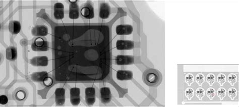
Traditional inspection methods, such as visual inspection or electrical testing, may not be sufficient to detect all of these defects, particularly those that are hidden within the layers of a multi-layer PCB. This is where X-ray inspection comes into play.

How Does X-ray Inspection Work?
X-ray inspection relies on the principle of X-ray attenuation. When X-rays pass through an object, they are absorbed or scattered differently depending on the material’s density and thickness. This difference in attenuation allows for the creation of an image that reveals the internal structure of the object.
In PCB inspection, X-rays are generated by an X-ray tube and directed towards the PCB. As the X-rays pass through the board, they are attenuated by the various materials present, such as the substrate, copper traces, and electronic components. The attenuated X-rays are then captured by a detector, which converts the signal into a digital image.
Types of X-ray Inspection Systems:
-
2D X-ray Inspection: This system produces a two-dimensional image of the PCB, providing a top-down view of the board’s internal structure. While useful for identifying some defects, it may not reveal all issues, particularly those related to the depth of solder joints or component placement.
-
3D X-ray Inspection (Computed Tomography): This advanced system takes multiple 2D X-ray images from different angles and uses computer processing to reconstruct a three-dimensional model of the PCB. This allows for a more comprehensive analysis of the board’s internal structure, revealing defects that may be hidden in a 2D image.
Advantages of X-ray Inspection:
- Non-destructive testing: X-ray inspection does not require any physical contact with the PCB, ensuring that the board remains intact and functional after the inspection process.
- Detecting hidden defects: X-ray inspection can reveal defects within the layers of a multi-layer PCB, such as voids, shorts, or misaligned components, which may not be visible through other inspection methods.
- Real-time monitoring: X-ray inspection can be integrated into the manufacturing process, allowing for real-time monitoring and early detection of defects, reducing waste and improving overall quality control.
- Detailed analysis: Advanced X-ray inspection systems can provide detailed measurements and analysis of solder joint quality, component placement, and other critical aspects of PCB Assembly.

Applications of X-ray Inspection in PCBs
X-ray inspection is widely used throughout the PCB manufacturing process, from prototype development to final product inspection. Some key applications include:
-
Prototype Validation: X-ray inspection can be used to validate the design and assembly of prototype PCBs, identifying any potential issues before moving into mass production.
-
Process Optimization: By monitoring the PCB assembly process with X-ray inspection, manufacturers can identify areas for improvement, such as adjusting solder paste application or component placement parameters.
-
Quality Control: X-ray inspection is an essential tool for final product quality control, ensuring that each PCB meets the required specifications and is free from defects that could lead to device failure.
-
Failure Analysis: In the event of a device failure, X-ray inspection can be used to analyze the PCB and identify the root cause of the issue, helping to prevent future occurrences and improve overall product reliability.

Challenges and Limitations of X-ray Inspection
Despite its many advantages, X-ray inspection is not without its challenges and limitations:
-
Cost: X-ray inspection systems, particularly advanced 3D systems, can be expensive to purchase and maintain, which may be a barrier for some manufacturers.
-
Operator Skill: Interpreting X-ray images and identifying defects requires skilled operators with specialized training and experience.
-
Radiation Safety: X-ray inspection involves the use of ionizing radiation, which can be harmful if not properly managed. Manufacturers must implement appropriate safety measures and training to protect operators and ensure compliance with regulations.
-
Material Limitations: Some materials, such as dense metals or certain types of components, may be difficult to penetrate with X-rays, limiting the effectiveness of the inspection process.
Despite these challenges, the benefits of X-ray inspection in ensuring PCB Quality and reliability make it an essential tool in modern electronics manufacturing.
Frequently Asked Questions (FAQ)
1. Is X-ray inspection safe for the PCBs being tested?
Yes, X-ray inspection is a non-destructive testing method, meaning that it does not damage or alter the PCB in any way. The low-energy X-rays used in the inspection process do not harm the electronic components or the board itself.
2. Can X-ray inspection detect all types of PCB defects?
While X-ray inspection is a powerful tool for identifying many types of defects, it may not detect all issues. Some defects, such as surface contamination or slight variations in trace width, may not be visible on an X-ray image. As such, X-ray inspection is often used in combination with other inspection methods, such as visual inspection or electrical testing, to ensure comprehensive quality control.
3. How long does X-ray inspection take?
The time required for X-ray inspection depends on various factors, such as the complexity of the PCB, the type of inspection system being used, and the level of analysis required. A basic 2D inspection may take only a few seconds per board, while a more advanced 3D computed tomography scan may take several minutes or more.
4. Can X-ray inspection be automated?
Yes, many modern X-ray inspection systems can be integrated into automated production lines, allowing for high-speed, continuous inspection of PCBs. Automated systems often use advanced image processing algorithms and machine learning techniques to identify defects and provide real-time feedback to the manufacturing process.
5. How much does an X-ray inspection system cost?
The cost of an X-ray inspection system can vary widely depending on factors such as the type of system (2D or 3D), the level of automation, and the specific features and capabilities required. Basic 2D systems may cost tens of thousands of dollars, while advanced 3D computed tomography systems can cost hundreds of thousands or even millions of dollars. However, the long-term benefits of improved quality control and reduced defect rates often justify the investment for many manufacturers.
| Characteristic | X-ray Inspection | Visual Inspection | Electrical Testing |
|---|---|---|---|
| Non-destructive | Yes | Yes | No |
| Detects hidden defects | Yes | No | Some |
| Real-time monitoring | Yes | Yes | Some |
| Detailed analysis | Yes | Limited | Some |
| Cost | High | Low | Moderate |
| Operator skill required | High | Moderate | Moderate |
| Limitations | Dense materials | Surface defects only | Some defects not detectable |
Conclusion
X-ray inspection is a powerful and essential tool in the manufacturing and quality control of printed circuit boards. By providing a non-destructive means of visualizing the internal structure of a PCB, X-ray inspection enables manufacturers to identify defects, optimize processes, and ensure the overall quality and reliability of their products.
As electronic devices continue to advance and miniaturize, the importance of X-ray inspection in PCB manufacturing will only continue to grow. Despite its challenges and limitations, the benefits of this technology make it an indispensable part of the modern electronics industry.


Leave a Reply