How Does Via-in-pad plating Work?
The via-in-pad plating process involves several key steps:
-
Via Drilling: First, holes are drilled through the PCB substrate at the locations where the vias will be placed. These holes are typically drilled using high-speed mechanical drills or laser drills, depending on the size and precision requirements of the vias.
-
Electroless Copper Deposition: Next, a thin layer of copper is deposited onto the walls of the via holes using an electroless plating process. This layer serves as a conductive seed layer for the subsequent electrolytic copper plating step.
-
Electrolytic Copper Plating: The PCB is then immersed in an electrolytic copper plating bath, where an electric current is applied to deposit a thicker layer of copper onto the walls of the via holes and the surface of the PCB. This step builds up the copper thickness to the desired level for electrical conductivity and mechanical strength.
-
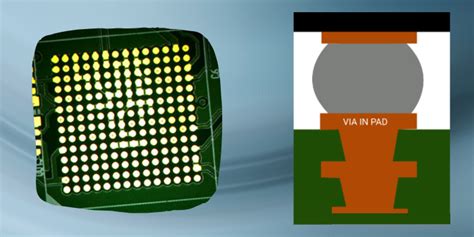
Pad Plating: After the via holes are plated, additional copper is plated onto the surface mount pads to create a raised “bumped” pad that is level with the top of the via. This ensures a smooth, flat surface for reliable soldering of surface mount components.
-
Finishing: Finally, a surface finish, such as immersion gold or organic solderability preservative (OSP), is applied to the plated vias and pads to protect the copper from oxidation and enhance solderability.
Advantages of Via-in-Pad Plating
Via-in-pad plating offers several key advantages over traditional PCB manufacturing techniques:
-
Space Savings: By placing vias directly in the surface mount pads, designers can save valuable board space and reduce the overall size of the PCB. This is particularly important for high-density designs with limited real estate.
-
Improved Signal Integrity: Via-in-pad plating minimizes the stub length of the via, which reduces the potential for signal reflections and improves overall signal integrity. This is critical for high-speed digital designs where signal quality is paramount.
-
Enhanced Mechanical Strength: The plated via provides additional mechanical support for the surface mount pad, which helps to prevent pad lifting or delamination during the soldering process.
-
Simplified Assembly: By creating a flat, bumped surface for component placement, via-in-pad plating simplifies the assembly process and improves the reliability of solder joints.
Challenges of Via-in-Pad Plating
Despite its many benefits, via-in-pad plating also presents some unique challenges that must be carefully managed:
-
Precise Drilling: The vias must be drilled with high precision to ensure proper alignment with the surface mount pads. Any misalignment can lead to incomplete plating or poor solder joint formation.
-
Consistent Plating Thickness: Achieving a consistent plating thickness across all the vias and pads on the PCB can be difficult, especially for high-aspect-ratio vias. Variations in plating thickness can impact electrical performance and reliability.
-
Thermal Management: The presence of plated vias in the surface mount pads can affect the thermal dissipation of the PCB, as the vias can act as heat sinks. Designers must carefully consider the thermal implications of via-in-pad plating and adjust their designs accordingly.
-
Cost: Via-in-pad plating typically involves additional processing steps compared to traditional PCB manufacturing, which can increase the overall cost of the PCB. However, the cost savings from reduced board size and improved reliability often outweigh the added manufacturing costs.

Applications of Via-in-Pad Plating
Via-in-pad plating is used in a wide range of electronic applications, including:
-
Smartphones and Tablets: The compact, high-density designs of modern mobile devices rely heavily on via-in-pad plating to maximize space utilization and ensure reliable connectivity.
-
Wearable Electronics: Smartwatches, fitness trackers, and other wearable devices use via-in-pad plating to achieve the smallest possible form factors without compromising performance.
-
Internet of Things (IoT) Devices: The proliferation of IoT devices, such as smart home sensors and industrial monitoring systems, has driven the need for compact, reliable PCBs that can be manufactured cost-effectively at scale.
-
Automotive Electronics: As vehicles become increasingly electrified and automated, the demand for high-performance, space-efficient PCBs has grown. Via-in-pad plating is used extensively in automotive applications such as advanced driver assistance systems (ADAS), infotainment systems, and power electronics.
-
Aerospace and Defense: The harsh environmental conditions and stringent reliability requirements of aerospace and defense applications make via-in-pad plating an essential technique for ensuring the long-term performance and durability of electronic systems.
Real-World Example: Apple iPhone
One of the most prominent examples of via-in-pad plating in consumer electronics is the Apple iPhone. As each new generation of iPhone has pushed the boundaries of performance and functionality, Apple’s engineers have relied on advanced PCB manufacturing techniques like via-in-pad plating to pack more features into smaller spaces.
The iPhone’s main logic board, which houses the A-series processor, memory, and other critical components, is a marvel of high-density PCB design. By using via-in-pad plating, Apple has been able to create an incredibly compact, multi-layer board that maximizes space utilization while ensuring reliable connectivity between components.
In addition to the main logic board, via-in-pad plating is used extensively throughout the iPhone’s subsystems, such as the camera module, touch screen controller, and wireless communication modules. By leveraging this advanced manufacturing technique, Apple has been able to consistently deliver cutting-Edge Performance and functionality in a sleek, pocket-friendly form factor.

Frequently Asked Questions (FAQ)
-
Q: What is the difference between via-in-pad and traditional vias?
A: Traditional vias are placed in the spaces between surface mount pads, while via-in-pad plating places the vias directly in the pads themselves. This allows for more efficient use of board space and improved signal integrity. -
Q: Can via-in-pad plating be used with both through-hole and blind/buried vias?
A: Yes, via-in-pad plating can be used with all types of vias, including through-hole vias that go completely through the PCB and blind/buried vias that only connect inner layers. -
Q: Is via-in-pad plating suitable for high-current applications?
A: Via-in-pad plating can be used for high-current applications, but designers must carefully consider the current-carrying capacity of the plated vias and adjust the via size and plating thickness accordingly. -
Q: How does via-in-pad plating affect the soldering process?
A: Via-in-pad plating creates a flat, bumped surface that is ideal for soldering surface mount components. The plated via provides additional mechanical support for the pad, reducing the risk of pad lifting or delamination during soldering. -
Q: Are there any special design considerations for via-in-pad plating?
A: Yes, designers must carefully consider the placement and size of the vias to ensure proper alignment with the surface mount pads. They must also account for the thermal implications of plated vias and adjust their designs to manage heat dissipation effectively.

Conclusion
Via-in-pad plating is a critical enabler of the compact, high-performance electronic devices that have become ubiquitous in our daily lives. By placing vias directly in surface mount pads, this advanced PCB manufacturing technique allows designers to maximize space utilization, improve signal integrity, and enhance the mechanical strength of solder joints.
While via-in-pad plating presents some unique challenges, such as precise drilling and consistent plating thickness, the benefits of this technique far outweigh the costs for a wide range of applications, from smartphones and wearables to automotive electronics and aerospace systems.
As electronic devices continue to evolve and push the boundaries of performance and functionality, via-in-pad plating will undoubtedly remain a vital tool in the PCB designer’s arsenal, enabling the creation of ever-smaller, more reliable, and more capable electronic systems.


Leave a Reply