Introduction
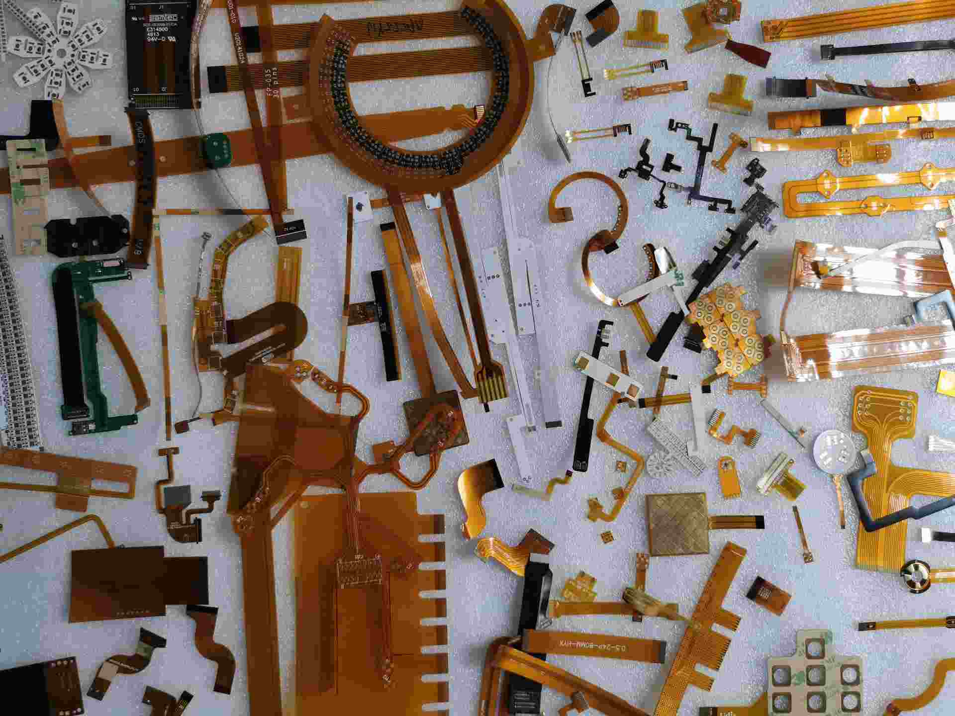
Flex PCBs, or flexible printed circuit boards, are thin and bendable circuit boards used in various electronic devices where rigid boards would be impractical. Flex PCBs allow circuits to flex and bend to fit inside small spaces within a device. As devices get smaller and more compact, there is a growing need to make flex PCBs even thinner while maintaining their flexibility and reliability. But how thin can flex PCBs actually get? This article will explore the limits of thinness for flex PCBs and discuss the thinnest flex PCB available today.
What are Flex PCBs?
A PCB, or printed circuit board, is a board made of fiberglass or other composite materials that provide mechanical support and electrical connectivity for electronic components using conductive copper traces etched from copper sheets laminated onto the substrate.
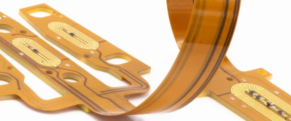
Traditional rigid PCBs are flat, stiff boards that cannot bend. Flex PCBs use highly flexible base materials that allow them to bend and flex. This flexibility allows flex PCBs to fold, twist, and wrap around components and fit into tight spaces where rigid boards would not work.
Some key properties of flex PCBs are:
- Thin, lightweight, and flexible substrate materials like polyimide. This allows bending without damage.
- Flexible conductive traces – usually copper. Can withstand repeated bending stress.
- No components soldered directly onto the PCB. Instead, components mount to rigid sections or attach with connectors.
- Can have portions that are rigid and portions that are flexible.
- Integrated connectivity to components and wires through traces etched from copper foil.
Flex PCBs are widely used in consumer electronics, medical devices, industrial equipment, aerospace applications, and more. Their thin, lightweight, and bendable nature allow them to fit into tight spaces and move dynamically in ways rigid boards cannot.
Why Make Flex PCBs Thinner?
There are a few key motivations for continuing to push flex PCBs to be thinner and thinner:
- Smaller and more compact devices: As consumer electronics like smartphones get smaller, there is less internal space available. Thinner flex PCBs allow more compact product designs.
- Lightweight: Thinner flex PCBs are also lighter. This is important in mobile devices and wearable technology where weight is a factor.
- High density: Thinner flex PCBs allow connections between components and high component densities even in tight spaces. More components in less space.
- Dynamic bending: Very thin flex PCBs can allow tighter dynamic bending radii for rollable, foldable, and shape-changing electronics.
- Cost savings: Thinner flex PCBs use less material, so they can reduce per unit costs.
As devices get smaller and more complex, there will be continued motivation to push flex PCBs thinner while maintaining performance and reliability.
How Thin can Flex PCBs Get?
So how thin can flex PCBs actually get? What are the limits of thinning flex PCBs before they lose functionality or become too fragile?
There are a few key factors that determine the functional lower limits of flex PCB thickness:
Minimum Trace Thickness
The conductive copper traces that carry current need to have a certain minimum thickness to effectively conduct electricity without overheating. Traces that are too thin can cause issues like:
- Increased resistivity leading to voltage drops
- Overheating of thin traces under current loads
- Higher likelihood of trace damage or breaks
In most applications, trace thickness on flex PCBs need to be at least around 15-20 microns to maintain performance. Trace thickness sets a lower bound on overall flex PCB thickness.
Minimum Substrate Thickness
The flexible substrate is the base material of the flex PCB that supports the traces. Polyimide is a common flexible substrate material. The substrate needs to have sufficient thickness for:
- Mechanical strength and durability
- Adequate trace adhesion to prevent delamination
- Sufficient heat tolerance and electrical isolation
The minimum substrate thickness is also typically around 15-20 microns. Thinner substrates often lack the strength and durability required for flex PCB longevity.
Minimum Bend Radius
Flex PCBs are designed to bend and flex. But there are limits to how tight their bend radius can get before traces crack or the substrate deforms plastically. Tighter bend radii require thicker flex PCBs for mechanical robustness.
Minimum bend radius is determined by things like:
- Substrate thickness
- Copper thickness
- Mechanical properties of base materials
In general, thinner flex PCBs have a larger minimum bend radius, limiting their flexibility.
Reliability and Lifetime
Thinner flex PCBs are inherently more fragile and prone to damage than thicker boards. They need to still maintain reliability over the lifetime of the product. Extremely thin flex PCBs may fail early due to:
- Trace cracking from repeated dynamic bending
- Breakage from vibrations or shock
- Pinholes and manufacturing defects
Sufficient thickness is required for reliable operation over decades in some cases.
What is the Thinnest Flex PCB Today?

Taking into account the various design constraints and manufacturing limitations outlined above, most flex PCBs end up in thickness ranges of around 50 to 150 microns for typical applications.
However, advances in materials science and manufacturing processes are allowing ever thinner flex PCBs to be produced:
- 25-50 microns – Some high end flex PCBs can be produced in thicknesses of 25 to 50 microns, pushing the boundaries of thinness while still maintaining functionality. This requires tightly controlled manufacturing to minimize defects and holes.
- 15-25 microns – On the leading edge, flex PCBs with thicknesses in the 15 to 25 micron range are becoming commercially available. These take special design consideration and embedded reinforcing structures to allow such thin substrates to survive bending and handling.
- Sub 15 microns – Research efforts have produced extremely thin flex PCBs under 15 microns in thickness. But these are not yet commercially viable for real-world applications. There are still challenges with reliability and manufacturability at this thickness level.
Mitsubishi Electric Flex PCBs
One company producing some of the thinnest commercially available flex PCBs today is Mitsubishi Electric. Some of their ultra-thin flex capabilities include:
- Availability of 25 micron total thickness products
- 12 micron polyimide substrate (most competitors use 25 micron minimum)
- Copper traces and spaces down to 15 microns (vs 25 micron typical minimum trace width)
This combination of thin substrate and high density traces allows Mitsubishi Electric to produce some of the thinnest functioning flex PCBs available. Their processes enable reliable flex PCBs thinner than 25 microns.
Discussion
In summary, while flex PCBs down to 15-25 microns are now commercially feasible, going below that thickness presently involves manufacturing and reliability tradeoffs that make them impractical for most real world applications.
As technology improves, we may continue to see the lower limits of flex PCB thickness pushed further. But for now, 25 microns appears to be nearing the functional lower bound for flexible PCBs with current materials and processes. Going thinner requires advances in material strength, defect reduction, and layered design among other areas.
Applications of Ultra-Thin Flex PCBs
What are some current and future applications where these ultra-thin flex PCBs provide unique advantages?
Wearable Electronics
For wearable devices like smart watches, smart glasses, fitness bands, and health monitoring devices, thin flexible PCBs are crucial for conforming to the body. Thinner flex PCBs allow more comfort and flexibility for the wearer. Flex PCBs under 50 microns are ideal for these applications.
Foldable Displays
Foldable displays, like foldable smartphones, require flex PCBs that can withstand extremely tight bend radii. Thinner flex PCBs down to 25 microns may eventually support fold radii down to 5 mm for compact folded state designs.
Medical Devices
Implantable medical devices like cochlear implants and glucose monitors need to be as compact and non-invasive as possible. Thin flex PCBs can help reduce the profiles of devices that integrate with the body.
Aerospace and Defense
In aerospace, thinner and lighter flex PCBs can reduce payload weight. Tight spaces in satellites and drones also require truly flexible boards. Ruggedized ultra-thin boards may find use in harsh defense environments.
Automotive
Automotive electronics and sensors need to operate reliably in demanding conditions, including vibration, shock, and temperature extremes. Thin flex PCBs are ideal for connecting components in tight spaces under the hood and in vehicle bodies.
As applications demand ever thinner and more nimble electronic assemblies, flex PCBs will continue advancing. While not yet ready for widespread adoption, flex PCBs at the cutting edge of 15-25 micron thickness pave the way for future electronics.
Manufacturing Processes for Ultra-Thin Flex PCBs
Producing ultra-thin flex PCBs requires specialized manufacturing processes and handling considerations. What are some key ways that ultra-thin flex PCB fabrication differs from standard thickness boards?
Tight Process Controls
Extremely tight control of material dimensions and etching processes is needed to achieve reliable circuits at 15-25 microns. Standard PCB fabrication tolerances are inadequate. Automated optical inspection and measurement ensures minimal variation.
Thin Dielectric Layers
Dielectric substrate materials like polyimide must be produced at thinner than normal dimensional targets, requiring specialized suppliers and tight supplier process controls.
Surface Treatment
Surface treatments may be used to increase adhesion and reduce delamination risks when using ultra-thin laminates and copper foils.
Special Handling
Such thin boards require delicate handling during fabrication, transportation, and assembly to prevent damage. Automated material handling is preferred. Boards may be left partially reinforced in panels for easier handling.
Minimized Defects
Even tiny defects like pinholes can compromise electrical isolation on ultra-thin boards. Manufacturing processes must minimize potential defects through cleanroom environments and rigorous quality control.
Advanced Testing
Electrical, mechanical, and functional testing methodologies tailored to ultra-thin flex PCBs verify that they meet application requirements before shipping. This may include flex testing and specialized inspection.
Reinforcement Structures
Strategic use of rigid sections, stiffeners, and selective reinforcement at connection points or high-stress areas helps protect the thin flexible circuits during assembly and use.
While producing high yields of ultra-thin flex PCBs is challenging, the potential benefits make the manufacturing efforts worthwhile for cutting-edge applications.
Challenges with Ultra-Thin Flex PCBs
Despite their advantages, ultra-thin flex PCBs down to 25 microns and below also come with some unique design and manufacturing challenges:
Fragility and Damage
The thin flexible boards are naturally fragile and prone to damage during handling, insertion, and assembly if not properly reinforced. Care must be taken to avoid cracking or creasing of traces.
Registration and Alignment
Precise registration and alignment of layers is critical but difficult with thin flexible substrates. Specialized laser drilling and optical alignment systems may be required.
Thermal Issues
Thinner copper and dielectric result in less effective heat spreading. Thermal management of components on ultra-thin flex PCBs requires careful design.
Tight Tolerances
Trace widths, spaces, and alignments must be held to tighter tolerances compared to standard flex PCBs, increasing cost and complexity.
Advanced Modeling
Thin flexible circuits require advanced modeling of factors like thermal behavior, dynamic bending stresses, vibration response, and fatigue over time.
Overall, moving to the extremes of thinness with flex PCBs involves overcoming significant technical hurdles. Careful design consideration and close partnership with specialized manufacturers can yield robust solutions.
Future Outlook
What does the future look like for continued advances in ultra-thin flex PCB technology? Here are some promising directions:
Novel Substrate Materials
Development of flexible substrate materials with properties tuned for ultra-thin applications. Examples include liquid crystal polymers and advanced polyimides.
Additive Processing
Additive fabrication techniques like inkjet and aerosol printing allow deposition of traces in the exact required patterns without etching. This avoids the need for thick copper foils.
3D Structures
Incorporation of 3D structural designs and shapes beyond simple flat flex PCBs. This provides mechanical reinforcement and flexibility tuned to the application.
Embedded Components
Embedding bare die components directly into ultra-thin flex PCBs to minimize overall package size and maximize performance.
Stretchable Circuits
Development of stretchable conductors and elastomers enable truly flexible and shape-reforming PCBs.
Laser Processing
Lasers allow precision micro-machining of ultra-thin substrates for etching, cutting, and drilling through tight process control.
The next generation of thin flex PCB technology will open doors for applications we can’t yet imagine. It’s an exciting time for pushing the boundaries of flexible hybrid electronics into the future.
Frequently Asked Questions
What is the main advantage of making flex PCBs thinner and thinner?
The main advantages are allowing electronics packages to become more compact and lightweight. Thinner flex PCBs take up less space and allow more compact product designs. They also weigh less, which is especially important in mobile devices.
How thin can flex PCBs get before they become too fragile?
In general, below about 25 microns, flex PCBs start to become too delicate for reliable functionality in most real-world conditions. Advanced handling and reinforcement is required to go below 20-25 microns for most applications.
Are there any performance tradeoffs with ultra-thin flex PCBs?
Yes, as flex PCBs get thinner, challenges can include lower current capacity, worse heat dissipation, smaller feature sizes, tighter tolerances, and more potential for damage. Careful design consideration is needed.
What new applications will ultra-thin flex PCBs enable?
Some key applications include wearable devices, compact foldable smartphones, flexible displays, minimally invasive medical devices, and lightweight drone/aerospace electronics.
What are some key ways thin flex PCB manufacturing differs from standard PCBs?
Key differences include tighter process control, thinner materials, surface treatments, delicate handling, minimized defects, advanced testing, and strategic reinforcement.
What technological advances will further enable thinner flex PCBs in the future?
Some promising directions are new substrate materials, additive printing, 3D structural designs, embedded components, stretchable circuits, and laser processing.


Leave a Reply