Introduction to PCB inspection
Printed Circuit Board (PCB) inspection is a crucial step in ensuring the quality and reliability of electronic products. The PCB incoming inspection process is designed to identify and eliminate defects, anomalies, and non-conformities in the PCBs before they are used in the manufacturing process. This comprehensive guide will delve into the various aspects of the PCB incoming inspection process, including the types of inspections, tools and techniques used, and best practices for effective quality control.
The Importance of PCB Inspection
PCB inspection plays a vital role in maintaining the quality and functionality of electronic devices. By identifying defects early in the manufacturing process, companies can:
- Reduce the risk of product failures and recalls
- Improve overall product quality and reliability
- Minimize production delays and associated costs
- Enhance customer satisfaction and brand reputation

Types of PCB Inspections
There are several types of PCB inspections performed during the incoming inspection process. Each type focuses on different aspects of the PCB to ensure comprehensive quality control.
1. Visual Inspection
Visual inspection is the most basic and essential type of PCB inspection. It involves examining the PCB with the naked eye or using magnifying tools to identify visible defects, such as:
- Scratches, dents, or cracks on the PCB surface
- Incorrect component placement or orientation
- Solder bridging or insufficient solder joints
- Contamination or foreign objects on the board
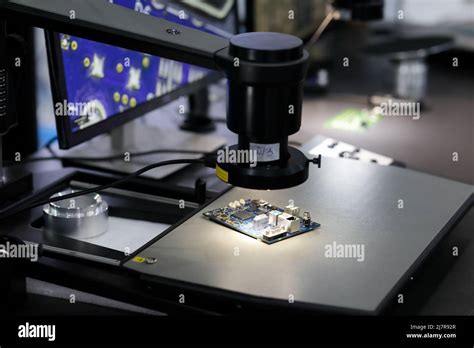
2. Automated Optical Inspection (AOI)
Automated Optical Inspection (AOI) uses advanced cameras and image processing software to detect surface-level defects on the PCB. AOI systems compare the captured images of the PCB to a pre-defined set of design specifications and identify any discrepancies. Some common defects detected by AOI include:
- Missing or misaligned components
- Incorrect component polarity
- Solder defects (e.g., bridging, insufficient solder, or solder balls)
- Trace or pad damage
3. X-Ray Inspection
X-ray inspection is used to examine the internal structure of the PCB, particularly for components with hidden or obscured solder joints, such as Ball Grid Arrays (BGAs) or Quad Flat No-leads (QFNs). X-ray inspection can detect:
- Voids or insufficient solder in hidden joints
- Misaligned or shifted components
- Broken or damaged internal traces or vias
4. Electrical Testing
Electrical testing verifies the functionality and performance of the PCB by checking for shorts, opens, and other electrical defects. There are two main types of electrical testing:
- In-Circuit Testing (ICT): Probes are used to test individual components and their connections on the PCB.
- Functional Testing (FCT): The PCB is tested as a complete system to ensure it performs according to its intended specifications.

Tools and Techniques Used in PCB Inspection
To perform effective PCB inspections, various tools and techniques are employed, depending on the type of inspection and the nature of the defects being targeted.
1. Magnification Tools
For visual inspections, magnification tools such as loupes, microscopes, or digital microscopes are used to enhance the visibility of small components and defects.
2. Lighting Techniques
Proper lighting is essential for accurate visual inspections. Different lighting techniques, such as bright field, dark field, or oblique lighting, can be used to highlight specific defects or features on the PCB.
3. Automated Inspection Systems
Automated inspection systems, such as AOI machines or X-ray inspection systems, use advanced imaging technology and software algorithms to detect and classify defects on the PCB. These systems can process large volumes of PCBs quickly and consistently, reducing the risk of human error.
4. Electrical Test Equipment
For electrical testing, specialized equipment such as in-circuit testers, flying probe testers, or boundary scan systems are used to verify the electrical connectivity and functionality of the PCB.

Best Practices for Effective PCB Inspection
To ensure a robust and effective PCB incoming inspection process, consider the following best practices:
- Establish clear quality standards and acceptance criteria based on industry guidelines and customer requirements.
- Train and certify inspection personnel to ensure consistent and accurate defect identification and classification.
- Implement a well-documented inspection procedure that outlines the steps, tools, and techniques to be used for each type of inspection.
- Regularly calibrate and maintain inspection equipment to ensure accurate and reliable results.
- Use statistical process control (SPC) techniques to monitor and analyze inspection data, identifying trends and opportunities for process improvement.
- Foster open communication and collaboration between the inspection team, suppliers, and internal stakeholders to address quality issues promptly and effectively.
PCB Inspection Sampling and Acceptance Quality Limit (AQL)
In many cases, it may not be practical or cost-effective to inspect every single PCB in a production lot. Instead, PCB inspection often relies on sampling techniques and Acceptance Quality Limit (AQL) standards to determine the acceptable level of defects in a lot.
AQL is a statistical method that defines the maximum number of defective units that can be accepted in a sample before the entire lot is rejected. The AQL level is typically determined based on the criticality of the PCB and the associated risk of defects.
Common AQL levels for PCB inspection include:
| AQL Level | Inspection Level | Acceptable Defects |
|---|---|---|
| 0.65% | II | 1 in 153 |
| 1.0% | II | 1 in 100 |
| 1.5% | II | 1 in 67 |
| 2.5% | II | 1 in 40 |
By using AQL sampling, companies can balance the cost and time of inspection with the acceptable level of risk for defective PCBs entering the production process.
Documenting and Reporting PCB Inspection Results
Proper documentation and reporting of PCB inspection results are essential for maintaining traceability, identifying trends, and driving continuous improvement efforts. An effective inspection report should include:
- PCB identification information (e.g., part number, revision, lot number)
- Inspection type and sampling plan used
- Detailed description and images of any defects found
- Defect classification and severity
- Disposition of the inspected PCBs (e.g., accepted, rejected, or reworked)
- Inspector information and date of inspection
Inspection reports should be stored in a centralized database and regularly reviewed by quality and engineering teams to identify patterns, root causes, and corrective actions for recurring defects.
Continuous Improvement of the PCB Inspection Process
To maintain a high level of quality and efficiency in the PCB incoming inspection process, continuous improvement efforts should be implemented. Some strategies for continuous improvement include:
- Regularly reviewing and updating inspection procedures and acceptance criteria based on new technologies, standards, and customer requirements.
- Investing in advanced inspection equipment and software to improve defect detection capabilities and inspection throughput.
- Providing ongoing training and certification for inspection personnel to keep their skills and knowledge up-to-date.
- Collaborating with suppliers to improve the quality of incoming PCBs and reduce the need for extensive inspections.
- Implementing a robust corrective action and preventive action (CAPA) system to address the root causes of recurring defects and prevent future occurrences.
Frequently Asked Questions (FAQ)
-
Q: What is the difference between AOI and X-ray inspection?
A: AOI (Automated Optical Inspection) uses cameras and image processing software to detect surface-level defects on the PCB, while X-ray inspection is used to examine the internal structure of the PCB, particularly for components with hidden or obscured solder joints. -
Q: How often should PCB inspection equipment be calibrated?
A: The frequency of calibration depends on the specific equipment and the manufacturer’s recommendations. Generally, inspection equipment should be calibrated at least annually or whenever there is a suspected issue with the accuracy of the results. -
Q: Can all PCB defects be detected through incoming inspection?
A: While incoming inspection is designed to catch a wide range of defects, it may not be possible to detect every single issue. Some defects, such as latent defects or intermittent failures, may only become apparent during functional testing or in the field. -
Q: What should be done with PCBs that fail incoming inspection?
A: PCBs that fail incoming inspection should be segregated from the accepted boards and clearly marked as defective. Depending on the nature and severity of the defects, the boards may be rejected, returned to the supplier, or reworked if feasible. -
Q: How can the cost of PCB inspection be justified?
A: While PCB inspection does add cost to the manufacturing process, it is essential for ensuring the quality and reliability of the final product. The cost of inspection should be weighed against the potential costs of product failures, recalls, and damage to brand reputation. Investing in effective PCB inspection can ultimately lead to cost savings by reducing scrap, rework, and warranty claims.
Conclusion
The PCB incoming inspection process is a critical step in ensuring the quality and reliability of electronic products. By implementing a comprehensive inspection strategy that includes visual inspection, AOI, X-ray inspection, and electrical testing, companies can identify and eliminate defects early in the manufacturing process, reducing the risk of product failures and associated costs.
Effective PCB inspection relies on well-defined procedures, skilled personnel, advanced tools and techniques, and a commitment to continuous improvement. By regularly reviewing and updating inspection processes, collaborating with suppliers, and investing in advanced technologies, companies can maintain a high level of quality control and stay competitive in today’s rapidly evolving electronics industry.


Leave a Reply